 |
Electronic Components Datasheet Search |
|
|
Electronic Components Datasheet Search |
|
The question interval is too short.
Please try again in a few seconds.

Hello, Please ask a question about BS170 Datasheet
# Example questions:
➢ What package dimensions are provided in the document, and what units are they presented in?
➢ What is the approximate turn-on time (ton) when the drain current (id) is 0.2 amps?
➢ How does increasing the junction temperature affect the gate-source threshold voltage (vgs(th))?
| Part No. | BS170 |
| Manufacturer | MOTOROLA |
| Size | 77 Kbytes |
| Pages | 4 pages |
| Description | TMOS FET Switching(N-Channel-Enhancement) |

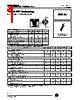



Document Type: Motorola Small-Signal Transistor Data Sheet (BS170/D)
Device: N-Channel Enhancement Mode Power MOSFET
1. Overview & Purpose
This document provides detailed specifications, electrical characteristics, switching characteristics, package dimensions, and application information for the Motorola BS170/D N-Channel Enhancement Mode Power MOSFET. It’s intended for engineers designing circuits that use this transistor.
2. Key Features & Characteristics
️· Enhancement Mode: The transistor is normally off and requires a gate voltage to turn on.
️· N-Channel: The transistor conducts when a positive voltage is applied to the gate relative to the source.
️· Power MOSFET: Designed to handle significant power and voltage levels.
️· Logic-Level Operation: Can be driven by standard logic circuits.
️· Fast Switching: Designed for switching applications.
3. Electrical Characteristics (Key Values)
️· V<sub>DS</sub> (Drain-Source Voltage): Up to 25V
️· V<sub>GS</sub>(th) (Gate-Source Threshold Voltage): 0.8V to 3.0V (Typically 2.0V) - Important for knowing the voltage needed to turn on the transistor.
️· r<sub>DS(on)</sub> (Drain-Source On Resistance): 1.8 Ω (Typically) – A lower value is desirable as it reduces power loss.
️· I<sub>D</sub>(off) (Drain Cutoff Current): 0.5µA – Indicates leakage current when the transistor is “off.”
️· gfs (Forward Transconductance): 200 mmhos – Relates drain current to gate-source voltage.
4. Switching Characteristics
️· t<sub>on</sub> (Turn-On Time): Up to 10 ns
️· t<sub>off</sub> (Turn-Off Time): Up to 10 ns
5. Package Information
️· Package Type: Not explicitly stated, but the package dimensions section provides information for a standard type.
️· Dimensions: The document includes detailed dimensional specifications in both inches and millimeters.
6. Figures and Diagrams (Important for understanding behavior)
️· Figure 6: Capacitance vs. Drain-Source Voltage: Shows how the capacitance of the transistor changes with the voltage between the drain and source. Important for high frequency designs.
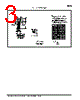
️· Figure 1: Switching Test Circuit: Illustrates the recommended setup for measuring switching characteristics.
️· Figure 2: Switching Waveforms: Visual representation of input and output signals during switching.
️· Figure 3: VGS(th) Normalized vs. Temperature: Shows how the gate threshold voltage changes with temperature.
️· Figure 4: On-Region Characteristics: A graphical representation of the relationship between voltage and current, with focus on the active region.
️· Figure 5: Output Characteristics: Graph of drain current versus drain-source voltage for various gate voltages.
7. Important Notes & Cautions
️· Power Dissipation: The document cautions that power dissipation can limit the maximum drain current. Proper heat sinking may be required.
️· Switching times: These values are maximums and will vary based on the driving circuit.
Document Type: Motorola Small-Signal Transistor Data Sheet (BS170/D)
Device: N-Channel Enhancement Mode Power MOSFET
1. Overview & Purpose
This document provides detailed specifications, electrical characteristics, switching characteristics, package dimensions, and application information for the Motorola BS170/D N-Channel Enhancement Mode Power MOSFET. It’s intended for engineers designing circuits that use this transistor.
2. Key Features & Characteristics
️· Enhancement Mode: The transistor is normally off and requires a gate voltage to turn on.
️· N-Channel: The transistor conducts when a positive voltage is applied to the gate relative to the source.
️· Power MOSFET: Designed to handle significant power and voltage levels.
️· Logic-Level Operation: Can be driven by standard logic circuits.
️· Fast Switching: Designed for switching applications.
3. Electrical Characteristics (Key Values)
️· V<sub>DS</sub> (Drain-Source Voltage): Up to 25V
️· V<sub>GS</sub>(th) (Gate-Source Threshold Voltage): 0.8V to 3.0V (Typically 2.0V) - Important for knowing the voltage needed to turn on the transistor.
️· r<sub>DS(on)</sub> (Drain-Source On Resistance): 1.8 Ω (Typically) – A lower value is desirable as it reduces power loss.
️· I<sub>D</sub>(off) (Drain Cutoff Current): 0.5µA – Indicates leakage current when the transistor is “off.”
️· gfs (Forward Transconductance): 200 mmhos – Relates drain current to gate-source voltage.
4. Switching Characteristics
️· t<sub>on</sub> (Turn-On Time): Up to 10 ns
️· t<sub>off</sub> (Turn-Off Time): Up to 10 ns
5. Package Information
️· Package Type: Not explicitly stated, but the package dimensions section provides information for a standard type.
️· Dimensions: The document includes detailed dimensional specifications in both inches and millimeters.
6. Figures and Diagrams (Important for understanding behavior)
️· Figure 6: Capacitance vs. Drain-Source Voltage: Shows how the capacitance of the transistor changes with the voltage between the drain and source. Important for high frequency designs.
️· Figure 1: Switching Test Circuit: Illustrates the recommended setup for measuring switching characteristics.
️· Figure 2: Switching Waveforms: Visual representation of input and output signals during switching.
️· Figure 3: VGS(th) Normalized vs. Temperature: Shows how the gate threshold voltage changes with temperature.
️· Figure 4: On-Region Characteristics: A graphical representation of the relationship between voltage and current, with focus on the active region.
️· Figure 5: Output Characteristics: Graph of drain current versus drain-source voltage for various gate voltages.
7. Important Notes & Cautions
️· Power Dissipation: The document cautions that power dissipation can limit the maximum drain current. Proper heat sinking may be required.
️· Switching times: These values are maximums and will vary based on the driving circuit.
| Part No. | BS170 |
| Manufacturer | MOTOROLA |
| Size | 77 Kbytes |
| Pages | 4 pages |
| Description | TMOS FET Switching(N-Channel-Enhancement) |
| Does ALLDATASHEET help your business so far? [ DONATE ] |
About Alldatasheet | Advertisement | Contact us | Privacy Policy | Link to Datasheet | Link Exchange | Manufacturer List All Rights Reserved©Alldatasheet.com |
| Russian : Alldatasheetru.com | Korean : Alldatasheet.co.kr | Spanish : Alldatasheet.es | French : Alldatasheet.fr | Italian : Alldatasheetit.com Portuguese : Alldatasheetpt.com | Polish : Alldatasheet.pl | Vietnamese : Alldatasheet.vn Indian : Alldatasheet.in | Mexican : Alldatasheet.com.mx | British : Alldatasheet.co.uk | New Zealand : Alldatasheet.co.nz |
|
Family Site : ic2ic.com |
icmetro.com |
 English ▼
  Chinese
 German
 Japanese
 Russian
 Korean
 Spanish
 French
 Italian
 Portuguese
 Polish
 Vietnamese
 Indian
 Mexican
 British
 New Zealand