|
Electronic Components Datasheet Search |
|
|
Electronic Components Datasheet Search |
|
IS25LP032D-RGLA3 Datasheet(PDF) 30 Page - Integrated Silicon Solution, Inc |
|
|
|||||||||||||||||||||||||||||
IS25LP032D-RGLA3 Datasheet(HTML) 30 Page - Integrated Silicon Solution, Inc |
|
|
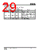
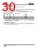
30 / 118 page  IS25LP032D IS25WP032D Integrated Silicon Solution, Inc.- www.issi.com 30 Rev. A12 08/04/2020 7. PROTECTION MODE The device supports hardware and software write-protection mechanisms. 7.1 HARDWARE WRITE PROTECTION The Write Protection (WP#) pin provides a hardware write protection method for BP3, BP2, BP1, BP0, SRWD, and QE in the Status Register. Refer to the section 6.1 STATUS REGISTER. Write inhibit voltage (VWI) is specified in the section 9.8 POWER-UP AND POWER-DOWN. All write sequence will be ignored when Vcc drops to VWI. Table 7.1 Hardware Write Protection on Status Register SRWD WP# Status Register 0 Low Writable 1 Low Protected 0 High Writable 1 High Writable Note: Before the execution of any program, erase or write Status Register instruction, the Write Enable Latch (WEL) bit must be enabled by executing a Write Enable (WREN) instruction. If the WEL bit is not enabled, the program, erase or write register instruction will be ignored. 7.2 SOFTWARE WRITE PROTECTION The device also provides a software write protection feature. The Block Protection (BP3, BP2, BP1, BP0) bits allow part or the whole memory area to be write-protected. |
|
Link URL |
| Does ALLDATASHEET help your business so far? [ DONATE ] |
About Alldatasheet | Advertisement | Contact us | Privacy Policy | Link to Datasheet | Link Exchange | Manufacturer List All Rights Reserved©Alldatasheet.com |
| Russian : Alldatasheetru.com | Korean : Alldatasheet.co.kr | Spanish : Alldatasheet.es | French : Alldatasheet.fr | Italian : Alldatasheetit.com Portuguese : Alldatasheetpt.com | Polish : Alldatasheet.pl | Vietnamese : Alldatasheet.vn Indian : Alldatasheet.in | Mexican : Alldatasheet.com.mx | British : Alldatasheet.co.uk | New Zealand : Alldatasheet.co.nz |
|
Family Site : ic2ic.com |
icmetro.com |
 English ▼
 English
 Chinese
 German
 Japanese
 Russian
 Korean
 Spanish
 French
 Italian
 Portuguese
 Polish
 Vietnamese
 Indian
 Mexican
 British
 New Zealand