|
Electronic Components Datasheet Search |
|
|
Electronic Components Datasheet Search |
|
TDA8559 Datasheet(PDF) 8 Page - NXP Semiconductors |
|
|
|||||||||||||||||||||||||||||
TDA8559 Datasheet(HTML) 8 Page - NXP Semiconductors |
|
|
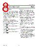
8 / 32 page  1997 Jun 27 8 Philips Semiconductors Product specification Low-voltage stereo headphone amplifier TDA8559 APPLICATION INFORMATION General For applications with a maximum supply voltage of 6 V (input mode LOW) the input pins need a DC path to ground (see Figs 3 and 4). For applications with supply voltages in the range from 6 to 18 V (input mode HIGH) the input DC level is 0.5VP + 0.6 V. In this situation the input configurations illustrated in Figs 5 and 6 have to be used. The capacitor Cb is recommended for stability improvement. The value may vary between 10 and 100 nF. This capacitor should be placed close to the IC between pin 12 and pin 13. Heatsink design The standard application is stereo headphone single-ended with a 32 Ω load impedance to buffer (see Fig.9). The headphone amplifier can deliver a peak output current of 150 mA into the load. For the DIP16 envelope Rth j-amb = 52 K/W; the maximum sine wave power dissipation for Tamb =25 °C is: For Tamb =60 °C the maximum total power dissipation is: For the SO16 envelope Rth j-amb = 105 K/W; the maximum sinewave power dissipation for Tamb =25 °C is: For Tamb =60 °C the maximum total power dissipation is: 2.4 W 150 25 – 52 ---------------------- = 1.7 W 150 60 – 52 ---------------------- = 1.2 W 150 25 – 105 ---------------------- = 0.85 W 150 60 – 105 ---------------------- = Test conditions Tamb =25 °C; unless otherwise specified: VP =3V, f = 1 kHz, RL =32 Ω, Gain = 26 dB, low input mode, band-pass filter: 22 Hz to 30 kHz. The total harmonic distortion as a function of frequency was measured with low-pass filter of 80 kHz. The quiescent current has been measured without any load impedance. In applications with coupling capacitors towards the load, an electrolytic capacitor has to be connected to pin 4 (SVRR). • The graphs for the single-ended application have been measured with the application illustrated in Fig.9; input configuration for input mode low (Fig.4) and input configuration for input mode high (Fig.6). • The graphs for the BTL application ‘input mode low’ have been measured with the application circuit illustrated in Fig.11 and the input configuration illustrated in Fig.4. • The graphs for the line-driver application have been measured with the application circuit illustrated in Fig.13 and the input configuration illustrated in Fig.6; input mode high. Input configurations The IC can be applied in two ways, ‘input mode low’ and ‘input mode high’. This can be selected by the input mode at pin 8: 1. Input mode low: pin 8 floating: The DC level of the input pins has to be between 0 V and (VP − 1.8 V). A DC path to ground is needed. The maximum output voltage is approximately 2.1 V (RMS). Input configurations illustrated in Figs 3 and 4 should be used. 2. Input mode high: pin 8 is connected to VP: This mode is intended for supply voltages >6 V. It can deliver a maximum output voltage of approximately 6 V (RMS) at THD = 0.5%. The DC voltage level of the input pins is (0.5VP + 0.6 V). Coupling capacitors are necessary. Input configurations illustrated in Figs 5 and 6 should be used. |
|
Link URL |
| Does ALLDATASHEET help your business so far? [ DONATE ] |
About Alldatasheet | Advertisement | Contact us | Privacy Policy | Link to Datasheet | Link Exchange | Manufacturer List All Rights Reserved©Alldatasheet.com |
| Russian : Alldatasheetru.com | Korean : Alldatasheet.co.kr | Spanish : Alldatasheet.es | French : Alldatasheet.fr | Italian : Alldatasheetit.com Portuguese : Alldatasheetpt.com | Polish : Alldatasheet.pl | Vietnamese : Alldatasheet.vn Indian : Alldatasheet.in | Mexican : Alldatasheet.com.mx | British : Alldatasheet.co.uk | New Zealand : Alldatasheet.co.nz |
|
Family Site : ic2ic.com |
icmetro.com |
 English ▼
 English
 Chinese
 German
 Japanese
 Russian
 Korean
 Spanish
 French
 Italian
 Portuguese
 Polish
 Vietnamese
 Indian
 Mexican
 British
 New Zealand