|
Electronic Components Datasheet Search |
|
|
Electronic Components Datasheet Search |
|
TC1303B-AO2EUNTR Datasheet(PDF) 20 Page - Microchip Technology |
|
|
|||||||||||||||||||||||||||||
TC1303B-AO2EUNTR Datasheet(HTML) 20 Page - Microchip Technology |
|
|
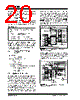
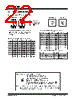
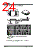
20 / 30 page  TC1303B DS21949A-page 20 © 2005 Microchip Technology Inc. As an example, for a 3.6V input, 1.8V output with a load of 400 mA, the efficiency taken from Figure 2-7 is approximately 84%. The internal power dissipation is approximately 171 mW. 5.6.2 LDO OUTPUT (VOUT2) The internal power dissipation within the TC1303B LDO is a function of input voltage, output voltage and output current. The following equation can be used to calculate the internal power dissipation for the LDO. EQUATION 5-7: The maximum power dissipation capability for a package can be calculated given the junction-to- ambient thermal resistance and the maximum ambient temperature for the application. The following equation can be used to determine the package’s maximum internal power dissipation. 5.6.3 LDO POWER DISSIPATION EXAMPLE 5.7 PCB Layout Information Some basic design guidelines should be used when physically placing the TC1303B on a Printed Circuit Board (PCB). The TC1303B has two ground pins, iden- tified as AGND (analog ground) and PGND (power ground). By separating grounds, it is possible to minimize the switching frequency noise on the LDO output. The first priority, while placing external compo- nents on the board, is the input capacitor (CIN1). Wiring should be short and wide; the input current for the TC1303B can be as high as 800 mA. The next priority would be the buck regulator output capacitor (COUT1) and inductor (L1). All three of these components are placed near their respective pins to minimize trace length. The CIN1 and COUT1 capacitor returns are con- nected closely together at the PGND plane. The LDO optional input capacitor (CIN2) and LDO output capaci- tor COUT2 are returned to the AGND plane. The analog ground plane and power ground plane are connected at one point (shown near L1). All other signals (SHDN1, SHDN2, feedback in the adjustable output case) should be referenced to AGND and have the AGND plane underneath them. FIGURE 5-1: Component Placement, Fixed 10-Pin MSOP. There will be some difference in layout for the 10-pin DFN package due to the thermal pad. A typical fixed- output DFN layout is shown below. For the DFN layout, the VIN1 to VIN2 connection is routed on the bottom of the board around the TC1303B thermal pad. FIGURE 5-2: Component Placement, Fixed 10-Pin DFN. Input Voltage VIN =5V±10% LDO Output Voltage and Current VOUT =3.3V IOUT =300 mA Internal Power Dissipation PLDO(MAX) =(VIN(MAX) – VOUT(MIN)) x IOUT(MAX) PLDO = (5.5V) – (0.975 x 3.3V)) x 300 mA PLDO =684.8 mW P LDO V IN MAX ) () VOUT2 MIN () – () I OUT2 MAX ) () × = Where: PLDO = LDO Pass device internal power dissipation VIN(MAX) = Maximum input voltage VOUT(MIN)= LDO minimum output voltage TC1303B 1 2 6 8 7 9 10 5 4 3 +VOUT1 PGND +VIN1 AGND AGND +VOUT2 COUT1 CIN2 COUT2 CIN1 PGND Plane AGND Plane L1 AGND to PGND +VIN2 * CIN2 Optional - Via 1 2 6 8 7 9 10 5 4 3 +VOUT1 PGND +VIN1 AGND AGND +VOUT2 COUT1 CIN2 COUT2 CIN1 PGND Plane AGND Plane L1 AGND to PGND PGND * CIN2 Optional +VIN2 TC1303B - Via |
|
Link URL |
| Does ALLDATASHEET help your business so far? [ DONATE ] |
About Alldatasheet | Advertisement | Contact us | Privacy Policy | Link to Datasheet | Link Exchange | Manufacturer List All Rights Reserved©Alldatasheet.com |
| Russian : Alldatasheetru.com | Korean : Alldatasheet.co.kr | Spanish : Alldatasheet.es | French : Alldatasheet.fr | Italian : Alldatasheetit.com Portuguese : Alldatasheetpt.com | Polish : Alldatasheet.pl | Vietnamese : Alldatasheet.vn Indian : Alldatasheet.in | Mexican : Alldatasheet.com.mx | British : Alldatasheet.co.uk | New Zealand : Alldatasheet.co.nz |
|
Family Site : ic2ic.com |
icmetro.com |
 English ▼
 English
 Chinese
 German
 Japanese
 Russian
 Korean
 Spanish
 French
 Italian
 Portuguese
 Polish
 Vietnamese
 Indian
 Mexican
 British
 New Zealand