|
Electronic Components Datasheet Search |
|
|
Electronic Components Datasheet Search |
|
TC1303C-AO2EMF Datasheet(PDF) 18 Page - Microchip Technology |
|
|
|||||||||||||||||||||||||||||
TC1303C-AO2EMF Datasheet(HTML) 18 Page - Microchip Technology |
|
|
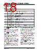
18 / 36 page  TC1303A/TC1303B/TC1303C/TC1304 DS21949B-page 18 © 2005 Microchip Technology Inc. 3.0 PIN DESCRIPTIONS The descriptions of the pins are listed in Table 3-1. TABLE 3-1: PIN FUNCTION TABLE 3.1 TC1303 LDO Shutdown Input Pin (SHDN2) SHDN2 is a logic-level input used to turn the LDO Reg- ulator on and off. A logic-high (> 45% of VIN), will enable the regulator output. A logic-low (< 15% of VIN) will ensure that the output is turned off. 3.2 TC1304 Shutdown Input Pin (SHDN) SHDN is a logic-level input used to initiate the sequenc- ing of the LDO output, then the buck regulator output. A logic-high (> 45% of VIN), will enable the regulator outputs. A logic-low (< 15% of VIN) will ensure that the outputs are turned off. 3.3 LDO Input Voltage Pin (VIN2) VIN2 is a LDO power input supply pin. Connect variable input voltage source to VIN2. Connect VIN1 and VIN2 together with board traces as short as possible. VIN2 provides the input voltage for the LDO. An additional capacitor can be added to lower the LDO regulator input ripple voltage. 3.4 LDO Output Voltage Pin (VOUT2) VOUT2 is a regulated LDO output voltage pin. Connect a 1 µF or larger capacitor to VOUT2 and AGND for proper operation. 3.5 Power-Good Output Pin (PG) PG is an output level indicating that VOUT2 (LDO) is within 94% of regulation. The PG output is configured as a push-pull for the TC1303B and open-drain output for the TC1303A, TC1303C and TC1304. 3.6 Analog Ground Pin (AGND) AGND is the analog ground connection. Tie AGND to the analog portion of the ground plane (AGND). See the physical layout information in Section 5.0 “Application Circuits/Issues” for grounding recommendations. 3.7 Buck Regulator Output Sense Pin (VFB/VOUT1) For VOUT1 adjustable-output voltage options, connect the center of the output voltage divider to the VFB pin. For fixed-output voltage options, connect the output of the buck regulator to this pin (VOUT1). 3.8 Buck Regulator Shutdown Input Pin (SHDN1) SHDN1 is a logic-level input used to turn the buck regulator on and off. A logic-high (> 45% of VIN), will enable the regulator output. A logic-low (< 15% of VIN) will ensure that the output is turned off. Pin No. TC1303 Name TC1304 Name Function 1 SHDN2 — Active Low Shutdown Input for LDO Output Pin 1 — SHDN Active Low Shutdown Input both Buck Regulator Output and LDO Output. Initiates sequencing up and down 2VIN2 VIN2 Analog Input Supply Voltage Pin 3VOUT2 VOUT2 LDO Output Voltage Pin 4 PG PG Power-Good Output Pin 5AGND AGND Analog Ground Pin 6VFB/VOUT1 VFB/VOUT1 Buck Feedback Voltage (Adjustable Version) / Buck Output Voltage (Fixed Version) Pin 7 SHDN1 — Active Low Shutdown Input for Buck Regulator Output Pin 7— AGND Analog Ground Pin 8VIN1 VIN1 Buck Regulator Input Voltage Pin 9LX LX Buck Inductor Output Pin 10 PGND PGND Power Ground Pin EP Exposed Pad Exposed Pad For the DFN package, the center exposed pad is a thermal path to remove heat from the device. Electrically this pad is at ground potential and should be connected to AGND |
|
Link URL |
| Does ALLDATASHEET help your business so far? [ DONATE ] |
About Alldatasheet | Advertisement | Contact us | Privacy Policy | Link to Datasheet | Link Exchange | Manufacturer List All Rights Reserved©Alldatasheet.com |
| Russian : Alldatasheetru.com | Korean : Alldatasheet.co.kr | Spanish : Alldatasheet.es | French : Alldatasheet.fr | Italian : Alldatasheetit.com Portuguese : Alldatasheetpt.com | Polish : Alldatasheet.pl | Vietnamese : Alldatasheet.vn Indian : Alldatasheet.in | Mexican : Alldatasheet.com.mx | British : Alldatasheet.co.uk | New Zealand : Alldatasheet.co.nz |
|
Family Site : ic2ic.com |
icmetro.com |
 English ▼
 English
 Chinese
 German
 Japanese
 Russian
 Korean
 Spanish
 French
 Italian
 Portuguese
 Polish
 Vietnamese
 Indian
 Mexican
 British
 New Zealand