|
Electronic Components Datasheet Search |
|
|
Electronic Components Datasheet Search |
|
WPCN384U Datasheet(PDF) 2 Page - Winbond |
|
|
|||||||||||||||||||||||||||||
WPCN384U Datasheet(HTML) 2 Page - Winbond |
|
|
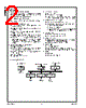
2 / 3 page  www.winbond.com 2 Revision 1.0 Features ■ Two Serial Ports (SP1 and SP2) — Software compatible with the 16550A and the 16450 — Shadow register support for write-only bit monitoring — UART data rates up to 1.5 Mbaud ■ IEEE 1284-Compliant Parallel Port — ECP, with Level 2 (14 mA sink and source output buffers) — Software or hardware control — Enhanced Parallel Port (EPP) compatible with EPP 1.7 and EPP 1.9 — Supports EPP as mode 4 of the Extended Control Register (ECR) — Selection of internal pull-up or pull-down resistor for Paper End (PE) pin — Supports a demand DMA mode mechanism and a DMA fairness mechanism for improved bus utilization — Protection circuit that prevents damage to the parallel port when a printer connected to it is pow- ered up or is operated at high voltages (in both cases, even if the WPCN384U is in power-down state) ■ 21 General-Purpose I/O (GPIO) Ports — Supports IRQ assertion — Programmable drive type for each output pin (open- drain, push-pull or output disable) — Programmable option for internal pull-up resistor on each input pin — Output lock option — Input debounce mechanism ■ LPC System Interface — 8-bit I/O cycles — LPCPD and CLKRUN support — Implements PCI mobile design guide recommenda- tion (PCI Mobile Design Guide 1.1, Dec. 18, 1998) ■ PC2001 and ACPI 3.0 Compliant — PnP Configuration Register structure — Flexible resource allocation for all logical devices ❏ Relocatable base address ❏ 15 IRQ routing options ❏ Optional 8-bit DMA channels (where applicable) selected from four possible DMA channels ■ Clock Sources — 14.318 MHz or 48 MHz clock input — LPC clock, 0 or 30 MHz to 33 MHz ■ Strap Configuration — Base Address (BADDR) strap to determine the base address of the Index-Data register pair — Strap Inputs to select testability mode ■ Power Supply — 3.3V supply operation — All pins are 5V tolerant, except LPC bus pins — All pins are back-drive protected, except LPC bus pins ■ Testability — XOR Tree — TRI-STATE device pins Internal Block Diagram Serial Port Bus Interface LPC Interface I/O Serial Port Serial Interface GPIO Ports Ports Parallel Port Interface Parallel Port IEEE 1284 14.31818 MHz Clock Generator 48 MHz Serial Interface |
|
|
Link URL |
| Does ALLDATASHEET help your business so far? [ DONATE ] |
About Alldatasheet | Advertisement | Contact us | Privacy Policy | Link to Datasheet | Link Exchange | Manufacturer List All Rights Reserved©Alldatasheet.com |
| Russian : Alldatasheetru.com | Korean : Alldatasheet.co.kr | Spanish : Alldatasheet.es | French : Alldatasheet.fr | Italian : Alldatasheetit.com Portuguese : Alldatasheetpt.com | Polish : Alldatasheet.pl | Vietnamese : Alldatasheet.vn Indian : Alldatasheet.in | Mexican : Alldatasheet.com.mx | British : Alldatasheet.co.uk | New Zealand : Alldatasheet.co.nz |
|
Family Site : ic2ic.com |
icmetro.com |
 English ▼
 English
 Chinese
 German
 Japanese
 Russian
 Korean
 Spanish
 French
 Italian
 Portuguese
 Polish
 Vietnamese
 Indian
 Mexican
 British
 New Zealand