|
Electronic Components Datasheet Search |
|
|
Electronic Components Datasheet Search |
|
FM1106-GA Datasheet(PDF) 4 Page - Ramtron International Corporation |
|
|
|||||||||||||||||||||||||||||
FM1106-GA Datasheet(HTML) 4 Page - Ramtron International Corporation |
|
|
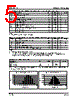
4 / 8 page  FM1106 - Automotive Temp. Rev. 3.0 Apr. 2009 Page 4 of 8 Electrical Specifications Absolute Maximum Ratings Symbol Description Ratings VDD Power Supply Voltage with respect to VSS -1.0V to +5.0V VIN Voltage on any signal pin with respect to VSS -1.0V to +5.0V and VIN < VDD+1.0V TSTG Storage temperature -55 °C to + 125°C TLEAD Lead temperature (Soldering, 10 seconds) 300 ° C VESD Electrostatic Discharge Voltage - Human Body Model (JEDEC Std JESD22-A114-B) - Charged Device Model (JEDEC Std JESD22-C101-A) - Machine Model (JEDEC Std JESD22-A115-A) 4kV 1kV 200V Package Moisture Sensitivity Level MSL-1 Stresses above those listed under Absolute Maximum Ratings may cause permanent damage to the device. This is a stress rating only, and the functional operation of the device at these or any other conditions above those listed in the operational section of this specification is not implied. Exposure to absolute maximum ratings conditions for extended periods may affect device reliability. DC Operating Conditions (TA = -40° C to +125° C, VDD = 2.7V to 3.6V unless otherwise specified) Symbol Parameter Min Typ Max Units Notes VDD Power Supply Voltage 2.7 - 3.6 V ISB Standby Current @ +85 °C @ +125 °C - - 5 8 µA µA 1 CPD Power Dissipation Capacitance - 165 pF 2 ILI Input Leakage Current ±1 µA 3 ILO Output Leakage Current ±1 µA 3 VIL Input Low Voltage -0.3 0.3 VDD V VIH Input High Voltage 0.7 VDD VDD + 0.3 V VOH Output High Voltage @ IOH = -1 mA VDD – 0.5 - V VOL Output Low Voltage @ IOL = 1 mA (VDD=2.7V) @ IOL = 10 mA (VDD=2.7V) - - 0.4 0.8 V V VHYS Input Hysteresis (CLK, EN) 200 mV 4 Notes 1. CLK = VSS, all other inputs at VDD or VSS. 2. To calculate device power dissipation, PD = CPD*VDD2*fi + CL*VDD2*fo, where fi is the input clk freq, fo is the output freq, and CL is the output load capacitance. Active current IDD may be calculated as IDD = CPD*VDD*fi, assuming outputs are floating. 3. VIN or VOUT = VSS to VDD. 4. This parameter is characterized but not tested. Capacitance (TA = 25° C , f=1.0 MHz, VDD = 3.3V) Symbol Parameter Min Max Units Notes CI Input Capacitance - 8 pF 1 Notes 1. This parameter is characterized but not tested. |
|
|
Link URL |
| Does ALLDATASHEET help your business so far? [ DONATE ] |
About Alldatasheet | Advertisement | Contact us | Privacy Policy | Link to Datasheet | Link Exchange | Manufacturer List All Rights Reserved©Alldatasheet.com |
| Russian : Alldatasheetru.com | Korean : Alldatasheet.co.kr | Spanish : Alldatasheet.es | French : Alldatasheet.fr | Italian : Alldatasheetit.com Portuguese : Alldatasheetpt.com | Polish : Alldatasheet.pl | Vietnamese : Alldatasheet.vn Indian : Alldatasheet.in | Mexican : Alldatasheet.com.mx | British : Alldatasheet.co.uk | New Zealand : Alldatasheet.co.nz |
|
Family Site : ic2ic.com |
icmetro.com |
 English ▼
 English
 Chinese
 German
 Japanese
 Russian
 Korean
 Spanish
 French
 Italian
 Portuguese
 Polish
 Vietnamese
 Indian
 Mexican
 British
 New Zealand