|
Electronic Components Datasheet Search |
|
|
Electronic Components Datasheet Search |
|
ADR3533WARMZ-R7 Datasheet(PDF) 15 Page - Analog Devices |
|
|
|||||||||||||||||||||||||||||
ADR3533WARMZ-R7 Datasheet(HTML) 15 Page - Analog Devices |
|
|
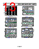
15 / 20 page  Data Sheet ADR3525/ADR3530/ADR3533/ADR3540/ADR3550 Rev. 0 | Page 15 of 20 0 1 2 3 4 5 6 7 8 9 RELATIVE SHIFT IN VOUT (%) Figure 33. Output Voltage Drift Distribution After Reflow (SHR Drift) 0 1 2 3 4 5 6 7 8 OUTPUT VOLTAGE HYSTERESIS (ppm) TA = +25°C → –40°C → +125°C → +25°C Figure 34. ADR3550 Thermally Induced Output Voltage Hysteresis Distribution 80 60 40 20 0 –20 –40 –60 –80 0 200 400 800 600 1000 ELAPSED TIME (Hours) Figure 35. ADR3550 Typical Long-Term Output Voltage Drift (Four Devices, 1000 Hours) |
|
|
Link URL |
| Does ALLDATASHEET help your business so far? [ DONATE ] |
About Alldatasheet | Advertisement | Contact us | Privacy Policy | Link to Datasheet | Link Exchange | Manufacturer List All Rights Reserved©Alldatasheet.com |
| Russian : Alldatasheetru.com | Korean : Alldatasheet.co.kr | Spanish : Alldatasheet.es | French : Alldatasheet.fr | Italian : Alldatasheetit.com Portuguese : Alldatasheetpt.com | Polish : Alldatasheet.pl | Vietnamese : Alldatasheet.vn Indian : Alldatasheet.in | Mexican : Alldatasheet.com.mx | British : Alldatasheet.co.uk | New Zealand : Alldatasheet.co.nz |
|
Family Site : ic2ic.com |
icmetro.com |
 English ▼
 English
 Chinese
 German
 Japanese
 Russian
 Korean
 Spanish
 French
 Italian
 Portuguese
 Polish
 Vietnamese
 Indian
 Mexican
 British
 New Zealand