|
Electronic Components Datasheet Search |
|
|
Electronic Components Datasheet Search |
|
AD5452 Datasheet(PDF) 12 Page - Analog Devices |
|
|
|||||||||||||||||||||||||||||
AD5452 Datasheet(HTML) 12 Page - Analog Devices |
|
|
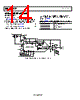
12 / 20 page  AD5547/AD5557 Data Sheet Rev. D | Page 12 of 20 CIRCUIT OPERATION DAC SECTION The AD5547/AD5557 are 16-/14-bit, multiplying, current- output, parallel input DACs. The devices operate from a single 2.7 V to 5.5 V supply and provide both unipolar (0 V to –VREF or 0 V to +VREF) and bipolar (±VREF) output ranges from –18 V to +18 V references. In addition to the precision conversion RFB commonly found in current output DACs, there are three addi- tional precision resistors for 4-quadrant bipolar applications. The AD5547/AD5557 consist of two groups of precision R-2R ladders, which make up the 12/10 LSBs, respectively. Furthermore, the 4 MSBs are decoded into 15 segments of resistor value 2R. Figure 18 shows the architecture of the 16-bit AD5547. Each of the 16 segments and the R-2R ladder carries an equally weighted current of one-sixteenth of full scale. The feedback resistor RFB and 4-quadrant resistor ROFS have values of 10 kΩ. Each 4-quadrant resistor, R1 and R2, equals 5 kΩ. In 4-quadrant operation, R1, R2, and an external op amp work together to invert the reference voltage and apply it to the VREF input. With ROFS and RFB connected as shown in Figure 2, the output can swing from −VREF to +VREF. The reference voltage inputs exhibit a constant input resistance of 5 kΩ ± 20%. The impedance of IOUT, the DAC output, is code dependent. External amplifier choice should take into account the variation of the AD5547/AD5557 output impedance. The feedback resistance in parallel with the DAC ladder resistance dominates output voltage noise. To maintain good analog performance, it is recommended that the power supply is bypassed with a 0.01 µF to 0.1 µF ceramic or chip capacitor in parallel with a 1 µF tantalum capacitor. Also, to minimize gain error, PCB metal traces between VREF and RFB should match. Every code change of the DAC corresponds to a step function; gain peaking at each output step may occur if the op amp has limited GBP and excessive parasitic capacitance present at the inverting node of the op amp. A compensation capacitor, therefore, may be needed between the I-to-V op amp inverting and output nodes to smooth the step transition. Such a compensation capacitor should be found empirically, but a 20 pF capacitor is generally adequate for the compensation. The VDD power is used primarily by the internal logic to drive the DAC switches. Note that the output precision degrades if the operating voltage falls below the specified voltage. Users should also avoid using switching regulators because device power supply rejection degrades at higher frequencies. 2R 80kΩ R 40kΩ 2R 80kΩ 2R 80kΩ 2R 80kΩ 2R 80kΩ 2R 80kΩ R 40kΩ 2R 80kΩ R 2R 80kΩ R 2R 80kΩ R 2R 80kΩ R 2R 80kΩ 2R 80kΩ R 40kΩ R2 5kΩ R1 5kΩ VREF 2R 80kΩ R 40kΩ 2R 80kΩ R 40kΩ 2R 80kΩ R 40kΩ 2R 80kΩ R 40kΩ 2R 80kΩ R 40kΩ 2R 80kΩ RCOM R1 ADDRESS DECODER DAC REGISTER INPUT REGISTER LDAC WR RS RS 4 MSB 15 SEGMENTS 8-BIT R2R 4-BIT R2R 15 8 4 LDAC WR D15 D14 D0 RS 10kΩ 10kΩ ROFS RFB IOUT AGND RA RB Figure 18. 16-Bit AD5547 Equivalent R-2R DAC Circuit with Digital Section, One Channel Shown |
|
|
Link URL |
| Does ALLDATASHEET help your business so far? [ DONATE ] |
About Alldatasheet | Advertisement | Contact us | Privacy Policy | Link to Datasheet | Link Exchange | Manufacturer List All Rights Reserved©Alldatasheet.com |
| Russian : Alldatasheetru.com | Korean : Alldatasheet.co.kr | Spanish : Alldatasheet.es | French : Alldatasheet.fr | Italian : Alldatasheetit.com Portuguese : Alldatasheetpt.com | Polish : Alldatasheet.pl | Vietnamese : Alldatasheet.vn Indian : Alldatasheet.in | Mexican : Alldatasheet.com.mx | British : Alldatasheet.co.uk | New Zealand : Alldatasheet.co.nz |
|
Family Site : ic2ic.com |
icmetro.com |
 English ▼
 English
 Chinese
 German
 Japanese
 Russian
 Korean
 Spanish
 French
 Italian
 Portuguese
 Polish
 Vietnamese
 Indian
 Mexican
 British
 New Zealand