|
Electronic Components Datasheet Search |
|
|
Electronic Components Datasheet Search |
|
MP7542JS Datasheet(PDF) 6 Page - Exar Corporation |
|
|
|||||||||||||||||||||||||||||
MP7542JS Datasheet(HTML) 6 Page - Exar Corporation |
|
|
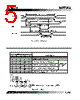
6 / 12 page  MP7542 6 Rev. 2.00 APPLICATION NOTES Refer to Section 8 for Applications Information Interface Logic Information The MP7542 is designed to interface as a memory-mapped output device. A typical system configuration is shown below. CS is the de- coded device address, and is derived by decoding the 14 higher order address bits. A0 and A1 are the MP7542 operation ad- dress bits, and are decoded internally in the MP7542 to point to the desired loading operation (i.e. load high byte, middle byte, low byte or DAC register). See Table 1. All data loading operations are identical to the write cycle of a RAM. Additionally, the CLR input allows the MP7542 DAC register to be cleared asynchronously to 0000 0000 0000. When operat- ing the MP7542 in a unipolar mode a CLEAR sets the DAC out- put to zero scale output. In the bipolar mode a CLEAR causes the DAC output to go to –VREF. In summary: 1. The MP7542 DAC register can be asynchronously cleared with the CLR input. 2. Each MP7542 requires only 4 bits of memory. 3. Any of the four basic loading operations (i.e. load low byte data register, middle byte data register, high byte data register or 12-bit DAC register) are accomplished by executing a memory WRITE operation to the applica- ble address location for the required DAC operation. Figure 2. 8085/MP7542 Interface (Memory Mapped Output) ADDRESS BUS (16) A0-15 8212 MP7542 FROM SYSTEM RESET (8) AD0-7 DATA 8085 or comparable (8) ALE WR Address Decode ADDRESS (16) DATA (8) +5 V CLR DB3 DB2 DB1 DB0 A0 A1 AD0 AD1 AD2 AD3 ADDR ADDR/DATA DECODED A2 - 15 USED AS CHIP SELECT A2 - 15 A0 A1 WR CS |
|
|
Link URL |
| Does ALLDATASHEET help your business so far? [ DONATE ] |
About Alldatasheet | Advertisement | Contact us | Privacy Policy | Link to Datasheet | Link Exchange | Manufacturer List All Rights Reserved©Alldatasheet.com |
| Russian : Alldatasheetru.com | Korean : Alldatasheet.co.kr | Spanish : Alldatasheet.es | French : Alldatasheet.fr | Italian : Alldatasheetit.com Portuguese : Alldatasheetpt.com | Polish : Alldatasheet.pl | Vietnamese : Alldatasheet.vn Indian : Alldatasheet.in | Mexican : Alldatasheet.com.mx | British : Alldatasheet.co.uk | New Zealand : Alldatasheet.co.nz |
|
Family Site : ic2ic.com |
icmetro.com |
 English ▼
 English
 Chinese
 German
 Japanese
 Russian
 Korean
 Spanish
 French
 Italian
 Portuguese
 Polish
 Vietnamese
 Indian
 Mexican
 British
 New Zealand