|
Electronic Components Datasheet Search |
|
|
Electronic Components Datasheet Search |
|
M30620FCAFP Datasheet(PDF) 110 Page - Mitsubishi Electric Semiconductor |
|
|
|||||||||||||||||||||||||||||
M30620FCAFP Datasheet(HTML) 110 Page - Mitsubishi Electric Semiconductor |
|
|
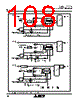
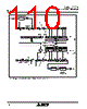
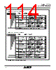
110 / 274 page  Mitsubishi microcomputers M16C / 62A Group SINGLE-CHIP 16-BIT CMOS MICROCOMPUTER Serial I/O 110 SP SP PAR 2SP 1SP UART UART (7 bits) UART (8 bits) UART(7 bits) UART (9 bits) Clock synchronous type Clock synchronous type Data bus low-order bits TxD2 UART2 transmit register PAR disabled PAR enabled D8 D7 D6 D5 D4 D3 D2 D1 D0 UART2 transmit buffer register UART (8 bits) UART (9 bits) Clock synchronous type UART2 receive buffer register UART2 receive register 2SP 1SP UART (7 bits) UART (8 bits) UART(7 bits) UART (9 bits) Clock synchronous type Clock synchronous type RxD2 UART (8 bits) UART (9 bits) Address 037E16 Address 037F16 Address 037A16 Address 037B16 Data bus high-order bits D7 D6 D5 D4 D3 D2 D1 D0 D8 000 0000 SP SP PAR “0” Reverse No reverse Error signal output circuit RxD data reverse circuit Error signal output enable Error signal output disable Reverse No reverse Logic reverse circuit + MSB/LSB conversion circuit Logic reverse circuit + MSB/LSB conversion circuit PAR enabled PAR disabled UART Clock synchronous type TxD data reverse circuit SP: Stop bit PAR: Parity bit Figure 1.16.3. Block diagram of UART2 transmit/receive unit |
|
Link URL |
| Does ALLDATASHEET help your business so far? [ DONATE ] |
About Alldatasheet | Advertisement | Contact us | Privacy Policy | Link to Datasheet | Link Exchange | Manufacturer List All Rights Reserved©Alldatasheet.com |
| Russian : Alldatasheetru.com | Korean : Alldatasheet.co.kr | Spanish : Alldatasheet.es | French : Alldatasheet.fr | Italian : Alldatasheetit.com Portuguese : Alldatasheetpt.com | Polish : Alldatasheet.pl | Vietnamese : Alldatasheet.vn Indian : Alldatasheet.in | Mexican : Alldatasheet.com.mx | British : Alldatasheet.co.uk | New Zealand : Alldatasheet.co.nz |
|
Family Site : ic2ic.com |
icmetro.com |
 English ▼
 English
 Chinese
 German
 Japanese
 Russian
 Korean
 Spanish
 French
 Italian
 Portuguese
 Polish
 Vietnamese
 Indian
 Mexican
 British
 New Zealand