|
Electronic Components Datasheet Search |
|
|
Electronic Components Datasheet Search |
|
M30620FCAFP Datasheet(PDF) 123 Page - Mitsubishi Electric Semiconductor |
|
|
|||||||||||||||||||||||||||||
M30620FCAFP Datasheet(HTML) 123 Page - Mitsubishi Electric Semiconductor |
|
|
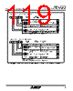
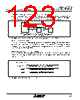
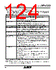
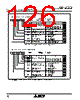
123 / 274 page  Mitsubishi microcomputers M16C / 62A Group SINGLE-CHIP 16-BIT CMOS MICROCOMPUTER Clock synchronous serial I/O mode 123 (c) Transfer clock output from multiple pins function (UART1) This function allows the setting two transfer clock output pins and choosing one of the two to output a clock by using the CLK and CLKS select bit (bits 4 and 5 at address 03B016). (See Figure 1.16.14.) The multiple pins function is valid only when the internal clock is selected for UART1. Figure 1.16.14. The transfer clock output from the multiple pins function usage Microcomputer TXD1 (P67) CLKS1 (P64) CLK1 (P65) IN CLK IN CLK Note: This applies when the internal clock is selected and transmission is performed only in clock synchronous serial I/O mode. (d) Continuous receive mode If the continuous receive mode enable bit (bits 2 and 3 at address 03B016, bit 5 at address 037D16) is set to “1”, the unit is placed in continuous receive mode. In this mode, when the receive buffer register is read out, the unit simultaneously goes to a receive enable state without having to set dummy data to the transmit buffer register back again. (e) Serial data logic switch function (UART2) When the data logic select bit (bit6 at address 037D16) = “1”, and writing to transmit buffer register or reading from receive buffer register, data is reversed. Figure 1.16.15 shows the example of serial data logic switch timing. Figure 1.16.15. Serial data logic switch timing D0 D1 D2 D3 D4 D5 D6 D7 D0 D1 D2 D3 D4 D5 D6 D7 Transfer clock TxD2 (no reverse) TxD2 (reverse) “H” “L” “H” “L” “H” “L” •When LSB first |
|
Link URL |
| Does ALLDATASHEET help your business so far? [ DONATE ] |
About Alldatasheet | Advertisement | Contact us | Privacy Policy | Link to Datasheet | Link Exchange | Manufacturer List All Rights Reserved©Alldatasheet.com |
| Russian : Alldatasheetru.com | Korean : Alldatasheet.co.kr | Spanish : Alldatasheet.es | French : Alldatasheet.fr | Italian : Alldatasheetit.com Portuguese : Alldatasheetpt.com | Polish : Alldatasheet.pl | Vietnamese : Alldatasheet.vn Indian : Alldatasheet.in | Mexican : Alldatasheet.com.mx | British : Alldatasheet.co.uk | New Zealand : Alldatasheet.co.nz |
|
Family Site : ic2ic.com |
icmetro.com |
 English ▼
 English
 Chinese
 German
 Japanese
 Russian
 Korean
 Spanish
 French
 Italian
 Portuguese
 Polish
 Vietnamese
 Indian
 Mexican
 British
 New Zealand