|
Electronic Components Datasheet Search |
|
|
Electronic Components Datasheet Search |
|
S-817B13AMC-CWC-T2 Datasheet(PDF) 17 Page - Seiko Instruments Inc |
|
|
|||||||||||||||||||||||||||||
S-817B13AMC-CWC-T2 Datasheet(HTML) 17 Page - Seiko Instruments Inc |
|
|
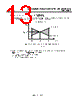
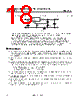
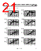
17 / 50 page  SUPER-SMALL PACKAGE CMOS VOLTAGE REGULATOR Rev.3.0_00 S-817 Series Seiko Instruments Inc. 17 The S-817 Series can be configured as a constant current circuit. Refer to Figure 15 and 16. Constant amperage (IO) is calculated using the following equation (VOUT(E): Effective output voltage): IO = (VOUT(E) ÷ RL) +ISS. Please note that it is impossible to set constant amperage IO in case of circuit (1) of Figure 15 to the value exceeding the drive ability of the S-817. However, circuit (2) of Figure 16 is an example to set constant amperage to the value exceeding the drive ability of the S-817. Circuit (2) incorporates a current boosting circuit. The maximum input voltage of the constant current circuit is the value obtained by adding 10 V to voltage of the device (VO). It is not recommended to attach a capacitor between the S-817 power source VIN and VSS pin or between output VOUT and VSS pin because rush current flows at powering on. An example of input voltage between VIN and VO in circuit (2) vs. IO current characteristics VIN, VO pins, Input voltage - IO current S-817A11ANB, S-817B11AMC, Tr : 2SK1213Y, R1 : 1 k Ω, VO=2 V 0.00 0.10 0.20 0.30 0.40 0.50 0.60 1.4 1.6 1.8 2 2.2 2.4 VIN −VO(V) RL =1.83 Ω 2.2 Ω 2.75 Ω 3.67 Ω 5.5 Ω 11 Ω |
|
Link URL |
| Does ALLDATASHEET help your business so far? [ DONATE ] |
About Alldatasheet | Advertisement | Contact us | Privacy Policy | Link to Datasheet | Link Exchange | Manufacturer List All Rights Reserved©Alldatasheet.com |
| Russian : Alldatasheetru.com | Korean : Alldatasheet.co.kr | Spanish : Alldatasheet.es | French : Alldatasheet.fr | Italian : Alldatasheetit.com Portuguese : Alldatasheetpt.com | Polish : Alldatasheet.pl | Vietnamese : Alldatasheet.vn Indian : Alldatasheet.in | Mexican : Alldatasheet.com.mx | British : Alldatasheet.co.uk | New Zealand : Alldatasheet.co.nz |
|
Family Site : ic2ic.com |
icmetro.com |
 English ▼
 English
 Chinese
 German
 Japanese
 Russian
 Korean
 Spanish
 French
 Italian
 Portuguese
 Polish
 Vietnamese
 Indian
 Mexican
 British
 New Zealand