|
Electronic Components Datasheet Search |
|
|
Electronic Components Datasheet Search |
|
SC4437EVB Datasheet(PDF) 9 Page - Semtech Corporation |
|
|
|||||||||||||||||||||||||||||
SC4437EVB Datasheet(HTML) 9 Page - Semtech Corporation |
|
|
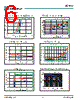
9 / 12 page  www.semtech.com © 2009 Semtech Corp. SC4437 9 Advantage Over Shunt References The SC4437 is a low power precision series voltage reference. The series reference has major advantages over shunt references when the load current has variations and the reference is powered by a battery. A shunt reference requires a resistance to connect the input and the output. This resistance will be designed to consume the maximum load current. When the actual load current is smaller than the maximum load current, the difference will be consumed by the reference. This behavior not only reduce efficiency but also increase the thermal stress on the device, thus is not desirable. On the contrary, the series reference consumes the same current as the load. When there is no load current required, the device itself consumes very little current (in the scale of 10s of µA). Precision Reference Over Wide Input Voltage Range, Load Conditions and Operating Temperatures The SC4437 can maintain 1% precision regulation over wide load range, operating temperature condition and input voltage range. To provide 3.3V output voltage, the load can range from 0 to 20mA; the temperature can range from -40 °C to 125 °C; the input voltage can range from V OUT + 0.9V to 28V, depending on the load and temperature conditions. The input voltage range should be selected based on the drop out voltage speci cation. Although the SC4437 can maintain tight regulation over wide operating conditions, attention should be paid to the thermal stress of the device. For example, with the input voltage of 28V and the load current of 20mA, the power consumption on the device is P = (28V-3.3V)*0.02A = 0.494W With the thermal resistance of 202 °C/W, the power consumption on the chip gives an ambient to junction temperature increase of 99.8 °C. If the ambient temperature is higher than 25 °C, then the junction temperature will be higher than 125°C, thus should be avoided. Input and Output Capacitances The SC4437 is stable with or without output capacitors under all load conditions. Adding output capacitances can improve the dynamic response under load transient. In order to obtain optimum performance under load transient, it is recommended that a 0.1 µF ceramic capacitor placed at the input and a 1 µF (and up) ceramic capacitor placed at the output. Reverse Battery Connection Protection The SC4437 has reverse battery connection protection. When the input and ground is reversely connected, the leakage current from the input is very small (maximum 6 µ A), protecting both the battery and the device itself. Load Transient Responses The following gure shows the circuit setup to test the 1 mA load transient response. 3.3V IN OUT GND SC4437 C IN 0.1 µF 5.8V (optional) C O 3.3V 2.3V 1 k Without output capacitance, the transient response is shown below. The high overshoot is due to the high resistance at high frequency without output capacitance. With 1µF capacitance, the transient response is improved signi cantly. The gure below shows the 1mA transient response with 1 µF capacitance at the output. Applications Information |
|
|
Link URL |
| Does ALLDATASHEET help your business so far? [ DONATE ] |
About Alldatasheet | Advertisement | Contact us | Privacy Policy | Link to Datasheet | Link Exchange | Manufacturer List All Rights Reserved©Alldatasheet.com |
| Russian : Alldatasheetru.com | Korean : Alldatasheet.co.kr | Spanish : Alldatasheet.es | French : Alldatasheet.fr | Italian : Alldatasheetit.com Portuguese : Alldatasheetpt.com | Polish : Alldatasheet.pl | Vietnamese : Alldatasheet.vn Indian : Alldatasheet.in | Mexican : Alldatasheet.com.mx | British : Alldatasheet.co.uk | New Zealand : Alldatasheet.co.nz |
|
Family Site : ic2ic.com |
icmetro.com |
 English ▼
 English
 Chinese
 German
 Japanese
 Russian
 Korean
 Spanish
 French
 Italian
 Portuguese
 Polish
 Vietnamese
 Indian
 Mexican
 British
 New Zealand