|
Electronic Components Datasheet Search |
|
|
Electronic Components Datasheet Search |
|
TMDS261B Datasheet(PDF) 9 Page - Texas Instruments |
|
|
|
|||||||||||||||||||||||||||||
TMDS261B Datasheet(HTML) 9 Page - Texas Instruments |
|
|
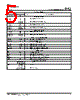
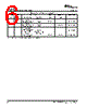
9 / 48 page  TMDS261B www.ti.com SLLS987A – SEPTEMBER 2009 – REVISED JULY 2011 DISSIPATION RATINGS DERATING FACTOR(1) TA = 70°C PACKAGE PCB JEDEC STANDARD TA ≤ 25°C ABOVE TA = 25°C POWER RATING Low-K 1066 mW 10.66 mW/ °C 586 mW 64-pin TQFP (PAG) High-K 1481 mW 14.8 mW/ °C 814 mW (1) This is the inverse of the junction-to-ambient thermal resistance when board-mounted and with no air flow. THERMAL CHARACTERISTICS over operating free-air temperature range (unless otherwise noted) PARAMETER TEST CONDITIONS MIN TYP MAX(1) UNIT RθJB Junction-to-board thermal resistance 37.13 °C/W RθJC Junction-to-case thermal resistance 15.3 °C/W Device power dissipation in normal LP = HIGH, TMDS: VID(pp) = 1200 mV, 3 Gbps PD(1) mode TMDS data pattern; HPD_SINK = HIGH, S1/S2 = 560 780 mW LOW/HIGH, HIGH/HIGH Device power dissipation in standby LP = HIGH, TMDS: VID(pp) = 1200 mV, 3 Gbps PD(2) mode TMDS data pattern; HPD_SINK = HIGH, S1 = HIGH, 10 20 mW S2 = LOW Device power dissipation in low-power PSD LP = LOW 1 2 mW mode Device power dissipation in normal LP = HIGH, no TMDS input clock, HPD_SINK = PNCLK 40 65 mW mode with no active TMDS input clock HIGH, S1/S2 = LOW/HIGH, HIGH/HIGH TJ Junction Temperature 0 125 °C (1) The maximum rating is simulated under 3.6-V VCC across worst-case temperature and process variation. Typical conditions are simulated at 3.3-V VCC, 25 °C with nominal process material. RECOMMENDED OPERATING CONDITIONS MIN NOM MAX UNIT VCC Supply voltage 3 3.3 3.6 V TA Operating free-air temperature 0 70 °C TMDS DIFFERENTIAL OUTPUT AND INPUT PINS VID(pp) Peak-to-peak input differential voltage 0.15 1.56 V VIC Input common-mode voltage VCC – 0.4 VCC + 0.01 V tIN_Rise_Fall TMDS input rise and fall time 75 ps Acceptable pre-emphasis on TMDS input signals. Note that an input signal VIN_PRE into TMDS261B with longer pre-emphasis duration and/or larger See (Figure 26) pre-emphasis ampltidue, could result in over-equalization. AVCC TMDS output termination voltage 3 3.3 3.6 V dR Data rate 3 Gbps RVSadj Resistor for TMDS-compliant voltage output swing 3.66 4.02 4.47 k Ω RT Termination resistance 45 50 55 Ω DDC PINS VI Input voltage 0 5.5 V dR(I2C) I2C data rate 100 Kbps HPD AND CONTROL PINS VIH High-level input voltage 2 5.5 V VIL Low-level input voltage 0 0.8 V Copyright © 2009–2011, Texas Instruments Incorporated 9 |
|
Link URL |
| Does ALLDATASHEET help your business so far? [ DONATE ] |
About Alldatasheet | Advertisement | Contact us | Privacy Policy | Link to Datasheet | Link Exchange | Manufacturer List All Rights Reserved©Alldatasheet.com |
| Russian : Alldatasheetru.com | Korean : Alldatasheet.co.kr | Spanish : Alldatasheet.es | French : Alldatasheet.fr | Italian : Alldatasheetit.com Portuguese : Alldatasheetpt.com | Polish : Alldatasheet.pl | Vietnamese : Alldatasheet.vn Indian : Alldatasheet.in | Mexican : Alldatasheet.com.mx | British : Alldatasheet.co.uk | New Zealand : Alldatasheet.co.nz |
|
Family Site : ic2ic.com |
icmetro.com |
 English ▼
 English
 Chinese
 German
 Japanese
 Russian
 Korean
 Spanish
 French
 Italian
 Portuguese
 Polish
 Vietnamese
 Indian
 Mexican
 British
 New Zealand