|
Electronic Components Datasheet Search |
|
|
Electronic Components Datasheet Search |
|
SMM665C Datasheet(PDF) 9 Page - Summit Microelectronics, Inc. |
|
|
|||||||||||||||||||||||||||||
SMM665C Datasheet(HTML) 9 Page - Summit Microelectronics, Inc. |
|
|
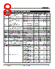
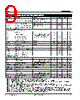
9 / 36 page  SMM665C Summit Microelectronics, Inc 2125 3.2 5/24/2011 9 DC OPERATING CHARACTERISTICS (CONTINUED) Symbol Parameter Notes Min Typ Max Unit VOUT_VALID Minimum Output Valid Voltage VDD_CAP voltage at which the PUP, RST, HEALTHY and FAULT outputs are valid 1 V UVLO UVLO (Under Voltage Lockout) threshold (Note 4) VDD_CAP rising 2.6 V VDD_CAP falling 2.5 V IVDD_CAP Maximum load on VDD_CAP, Note 10 10 mA AIN1/AIN2 ADC characteristics N Resolution 10 Bits MC Missing codes Minimum resolution for which no missing codes are guaranteed 10 Bits S/N Signal-to-noise Ratio Conversion rate = 500Hz 72 dB DNL Differential non-linearity -1/2 +1/2 LSB INL Integral non-linearity Note 7 -1 +1 LSB GAIN Positive full scale gain error Note 7 -0.5 ±0.16 +0.5 % OFFSET Offset error Note 7 -1 +1 LSB ADC_TC Full scale temperature coefficient ±15 ppm/ oC IMADC Analog ADC Input Impedance 10 M Ω IIVREF VREF input current 250 nA ICVREF VREF input capacitance 200 pF IRVREF VREF input impedance 1 k Ω VMA-VMF, VDD ADC characteristics N Resolution 10 Bits MC Missing codes Minimum resolution for which no missing codes are guaranteed 10 Bits S/N Signal-to-noise Ratio Conversion rate = 500Hz 72 dB ERR_ADC Total ADC Error Total ADC Read Error -4 +4 LSB IMADC Analog ADC Input Impedance VMA-VMF 100 K Ω 12VIN ADC characteristics N Resolution 10 Bits MC Missing codes Minimum resolution for which no missing codes are guaranteed 10 Bits S/N Signal-to-noise Ratio Conversion rate = 500Hz 72 dB ERR_ADC Total ADC Error Total ADC Read Error -4 +4 LSB Note 1 – Range depends on internal regulator set to 3.6V or 5.5V see 12VIN specification. Note 2 – See Application Note 37 which describes the type of capacitors to use to obtain minimum leakage. Note 3 – All logic levels are with respect to the voltage on VDD_CAP, when supplied from VDD; VDD_CAP is equal to VDD, under no load. Note 4 – (100mV typical Hysteresis) Note 5 – Under certain operating conditions, self-heating could result in additional temperature sensor error. Note 6 – SDA not included (separate electrical specification). The device can sink more than 20mA, however total ISINK from all PUPx pins should not exceed 6mA or ADOCACC specification will be affected. Note 7 – The formula for the total ADC inaccuracy is: [((ADC read voltage) +/- INL)*(range of gain error)]+range of offset error Note 8 – When temperature sensor is not used (determined by the hex file configuration setting) sensor accuracy is tested for typical values only. Note 9 – The term “FAULT#” throughout this document describes a pin and output signal, whereas the term “fault” describes an operating condition that may or may not activate the FAULT# pin. The FAULT# pin can only be activated by Ain1, Ain2 and Temperature fault conditions. Note 10 – Guaranteed by Design and/or Characterization – not 100% tested in production. |
|
Link URL |
| Does ALLDATASHEET help your business so far? [ DONATE ] |
About Alldatasheet | Advertisement | Contact us | Privacy Policy | Link to Datasheet | Link Exchange | Manufacturer List All Rights Reserved©Alldatasheet.com |
| Russian : Alldatasheetru.com | Korean : Alldatasheet.co.kr | Spanish : Alldatasheet.es | French : Alldatasheet.fr | Italian : Alldatasheetit.com Portuguese : Alldatasheetpt.com | Polish : Alldatasheet.pl | Vietnamese : Alldatasheet.vn Indian : Alldatasheet.in | Mexican : Alldatasheet.com.mx | British : Alldatasheet.co.uk | New Zealand : Alldatasheet.co.nz |
|
Family Site : ic2ic.com |
icmetro.com |
 English ▼
 English
 Chinese
 German
 Japanese
 Russian
 Korean
 Spanish
 French
 Italian
 Portuguese
 Polish
 Vietnamese
 Indian
 Mexican
 British
 New Zealand