|
Electronic Components Datasheet Search |
|
|
Electronic Components Datasheet Search |
|
TS3USB3200RSVR Datasheet(PDF) 11 Page - Texas Instruments |
|
|
|
|||||||||||||||||||||||||||||
TS3USB3200RSVR Datasheet(HTML) 11 Page - Texas Instruments |
|
|
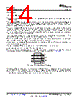
11 / 23 page  100Ω D+ D- MicroUSB Connector D+ D- ID_COM GND VBUS USB_DM DP DM ID USB+ USB- ID_USB VBUS MHL+ MHL- ID_MHL MHL+/MyDP+ MHL-/MyDP- CBUS/ID HDMI USB_DP UART_TX UART_RX SDA SCL INT VBAT Baseband or Application Processor TSU6111A HDMI to MHL/MyDP Bridge TS3USB3200 VBAT To Battery Charger SEL1 SEL2 VBUS ID GND PSEL VCC Copyright © 2016, Texas Instruments Incorporated 11 TS3USB3200 www.ti.com SCDS333B – JUNE 2012 – REVISED JULY 2016 Product Folder Links: TS3USB3200 Submit Documentation Feedback Copyright © 2012–2016, Texas Instruments Incorporated 8 Application and Implementation NOTE Information in the following applications sections is not part of the TI component specification, and TI does not warrant its accuracy or completeness. TI’s customers are responsible for determining suitability of components for their purposes. Customers should validate and test their design implementation to confirm system functionality. 8.1 Application Information For Mobility Display Port Applications (MyDP) the signal voltage must be biased to ensure that the signal never exceeds the Recommended Operating Conditions for the TS3USB3200. Namely the VI/O must never operate outside the range of 0 V to 3.6 V. The control pins (SEL1 and SEL2) have built-in 6-MΩ pulldown resistors to ensure the USB paths are enabled for TS3USB3200 and allow connectivity to the TSU5611 USB accessory switch. 8.2 Typical Applications 8.2.1 TS3USB3200 Configured to be Powered by VBUS Through the MicroUSB Connector During manufacturing test when battery power is not available, the TS3USB3200 can be configured, as shown in Figure 10, to be powered by VBUS through the microUSB connector. Figure 10. Typical Application Schematic Powered by VBUS 8.2.1.1 Design Requirements Design requirements of the MHL and USB 1.0,1.1, and 2.0 standards must be followed. The TS3USB3200 has internal 6-M Ω pulldown resistors on SEL and OE, so no external resistors are required on the logic pins. The internal pulldown resistor on SEL ensures the USB channel is selected by default. The internal pulldown resistor on OE enables the switch when power is applied to VCC. |
|
|
Link URL |
| Does ALLDATASHEET help your business so far? [ DONATE ] |
About Alldatasheet | Advertisement | Contact us | Privacy Policy | Link to Datasheet | Link Exchange | Manufacturer List All Rights Reserved©Alldatasheet.com |
| Russian : Alldatasheetru.com | Korean : Alldatasheet.co.kr | Spanish : Alldatasheet.es | French : Alldatasheet.fr | Italian : Alldatasheetit.com Portuguese : Alldatasheetpt.com | Polish : Alldatasheet.pl | Vietnamese : Alldatasheet.vn Indian : Alldatasheet.in | Mexican : Alldatasheet.com.mx | British : Alldatasheet.co.uk | New Zealand : Alldatasheet.co.nz |
|
Family Site : ic2ic.com |
icmetro.com |
 English ▼
 English
 Chinese
 German
 Japanese
 Russian
 Korean
 Spanish
 French
 Italian
 Portuguese
 Polish
 Vietnamese
 Indian
 Mexican
 British
 New Zealand