|
Electronic Components Datasheet Search |
|
|
Electronic Components Datasheet Search |
|
LM9831CCVJDX Datasheet(PDF) 10 Page - National Semiconductor (TI) |
|
|
|
|||||||||||||||||||||||||||||
LM9831CCVJDX Datasheet(HTML) 10 Page - National Semiconductor (TI) |
|
|
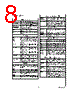
10 / 41 page  10 www.national.com LM9831 Register Listing Registers in bold boxes are reset to that value on power-up. All register addresses are in hexadecimal. All other numbers are decimal unless otherwise noted. Address Function D 7 D 6 D 5 D 4 D 3 D 2 D 1 D 0 Value IMAGE BUFFER (READ ONLY) 00 Pixel (Image) Data n n n n n n n n One byte of image data. STATUS REGISTERS (READ ONLY) 01 Image Data Available In Buffer nn nn nnn n n*2 (256k x 16 DRAM) or n*8 (1M x 16 DRAM) kilobytes of image data is available 02 PAPER SENSE 1 State read clears bit if edge sensitive input. 0False 1True PAPER SENSE 2 State read clears bit if edge sensitive input. 0False 1True MISC I/O 1 State read clears bit if edge sensitive input. 0False 1True MISC I/O 2 State read clears bit if edge sensitive input. 0False 1True MISC I/O 3 State read clears bit if edge sensitive input. 0False 1True MISC I/O 4 State read clears bit if edge sensitive input. 0False 1True MISC I/O 5 State read clears bit if edge sensitive input. 0False 1True MISC I/O 6 State read clears bit if edge sensitive input. 0False 1True DATAPORT REGISTERS 03 DataPort Target 0 0 Offset Coefficient Data 0 1 Gain Coefficient Data 1 0 Gamma Lookup Table 11 N/A DataPort Target Color 00 Red 0 1 Green 10 Blue 11 N/A Pause (Read Only) This bit indicates whether or not the scanner is currently paused due to a buffer full condition. 0 Normal State 1 The scanner is currently in the pause/reverse cycle. DRAM Test 0 Normal Operation 1 DRAM Test mode 04 DataPort Address - MSB R / W aa aaa a Address of location to be read/written to. a = 0 to 4095 for gamma tables, 0 to 16383 for Offset and Gain Coefficient Data Addresses greater than these are illegal. Bit D6 of register 4 indicates whether next operation will be a Read (D6=1) or a Write (D6=0). 05 DataPort Address - LSB aa aa aaa a 06 DataPort nn nn nnn n Data to be read from or written to the address of the currently selected Dataport Target. The DataPort Address is automatically incremented whenever one (gamma data) or two (Gain/Offset Data) bytes are read from or written to this register. |
|
Link URL |
| Does ALLDATASHEET help your business so far? [ DONATE ] |
About Alldatasheet | Advertisement | Contact us | Privacy Policy | Link to Datasheet | Link Exchange | Manufacturer List All Rights Reserved©Alldatasheet.com |
| Russian : Alldatasheetru.com | Korean : Alldatasheet.co.kr | Spanish : Alldatasheet.es | French : Alldatasheet.fr | Italian : Alldatasheetit.com Portuguese : Alldatasheetpt.com | Polish : Alldatasheet.pl | Vietnamese : Alldatasheet.vn Indian : Alldatasheet.in | Mexican : Alldatasheet.com.mx | British : Alldatasheet.co.uk | New Zealand : Alldatasheet.co.nz |
|
Family Site : ic2ic.com |
icmetro.com |
 English ▼
 English
 Chinese
 German
 Japanese
 Russian
 Korean
 Spanish
 French
 Italian
 Portuguese
 Polish
 Vietnamese
 Indian
 Mexican
 British
 New Zealand