|
Electronic Components Datasheet Search |
|
|
Electronic Components Datasheet Search |
|
M30620FCAFP Datasheet(PDF) 134 Page - Mitsubishi Electric Semiconductor |
|
|
|||||||||||||||||||||||||||||
M30620FCAFP Datasheet(HTML) 134 Page - Mitsubishi Electric Semiconductor |
|
|
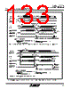
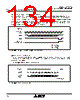
134 / 274 page  Mitsubishi microcomputers M16C / 62A Group SINGLE-CHIP 16-BIT CMOS MICROCOMPUTER Clock asynchronous serial I/O (UART) mode 134 (a) Function for outputting a parity error signal During reception, with the error signal output enable bit (bit 7 of address 037D16) assigned “1”, you can output an “L” level from the TXD2 pin when a parity error is detected. And during transmission, comparing with the case in which the error signal output enable bit (bit 7 of address 037D16) is as- signed “0”, the transmission completion interrupt occurs in the half cycle later of the transfer clock. Therefore parity error signals can be detected by a transmission completion interrupt program. Figure 1.16.23 shows the output timing of the parity error signal. Figure 1.16.23. Output timing of the parity error signal ST : Start bit P : Even Parity SP : Stop bit D0 D1 D2 D3 D4 D5 D6 D7 P SP ST Hi-Z Transfer clock RxD2 TxD2 Receive complete flag “H” “L” “H” “L” “H” “L” “1” • LSB first “0” (b) Direct format/inverse format Connecting the SIM card allows you to switch between direct format and inverse format. If you choose the direct format, D0 data is output from TxD2. If you choose the inverse format, D7 data is inverted and output from TxD2. Figure 1.16.24 shows the SIM interface format. Figure 1.16.24. SIM interface format P : Even parity D0 D1 D2 D3 D4 D5 D6 D7 P Transfer clcck TxD2 (direct) TxD2 (inverse) D7 D6 D5 D4 D3 D2 D1 D0 P |
|
Link URL |
| Does ALLDATASHEET help your business so far? [ DONATE ] |
About Alldatasheet | Advertisement | Contact us | Privacy Policy | Link to Datasheet | Link Exchange | Manufacturer List All Rights Reserved©Alldatasheet.com |
| Russian : Alldatasheetru.com | Korean : Alldatasheet.co.kr | Spanish : Alldatasheet.es | French : Alldatasheet.fr | Italian : Alldatasheetit.com Portuguese : Alldatasheetpt.com | Polish : Alldatasheet.pl | Vietnamese : Alldatasheet.vn Indian : Alldatasheet.in | Mexican : Alldatasheet.com.mx | British : Alldatasheet.co.uk | New Zealand : Alldatasheet.co.nz |
|
Family Site : ic2ic.com |
icmetro.com |
 English ▼
 English
 Chinese
 German
 Japanese
 Russian
 Korean
 Spanish
 French
 Italian
 Portuguese
 Polish
 Vietnamese
 Indian
 Mexican
 British
 New Zealand