|
Electronic Components Datasheet Search |
|
|
Electronic Components Datasheet Search |
|
LTM4612 Datasheet(PDF) 7 Page - Linear Technology |
|
|
|||||||||||||||||||||||||||||
LTM4612 Datasheet(HTML) 7 Page - Linear Technology |
|
|
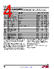
7 / 30 page  LTM4613 7 4613fd For more information www.linear.com/LTM4613 PIN FUNCTIONS VIN (Bank 1): Power Input Pins. Apply input voltage be- tween these pins and PGND pins. Recommend placing input decoupling capacitance directly between VIN pins and PGND pins. PGND (Bank 2): Power Ground Pins for Both Input and Output Returns. VOUT (Bank 3): Power Output Pins. Apply output load between these pins and PGND pins. Recommend placing output decoupling capacitance directly between these pins and PGND pins (see the LTM4613 Pin Configuration below). VD (Pins C1 to C7, B6 to B7, A6): Top FET Drain Pins. Add more high frequency ceramic decoupling capacitors between VD and PGND to handle the input RMS current and reduce the input ripple further. DRVCC(PinsC10,E11,E12):Thesepinsnormallyconnect to INTVCC for powering the internal MOSFET drivers. They can be biased up to 6V from an external supply with about 50mA capability. This improves efficiency at the higher inputvoltagesbyreducingpowerdissipationinthemodule. See the Applications Information section. INTVCC (Pin A7): This pin is for additional decoupling of the 5V internal regulator. PLLIN(PinA8):ExternalClockSynchronizationInputtothe Phase Detector. This pin is internally terminated to SGND with a 50k resistor. Apply a clock above 2V and below INTVCCsubjecttominimumon-timeandminimumoff-time requirements. See the Applications Information section. FCB (Pin M12): Forced Continuous Input. Connect this pin to SGND to force continuous synchronization operation at light load or to INTVCC to enable discontinuous mode operation at light load. TRACK/SS(PinA9):OutputVoltageTrackingandSoft-Start Pin. When the module is configured as a master output, then a soft-start capacitor is placed on this pin to ground to control the master ramp rate. A soft-start capacitor can be used for soft-start turn-on as a standalone regulator. Slave operation is performed by putting a resistor divider from the master output to the ground, and connecting the center point of the divider to this pin. See the Applications Information section. MPGM (Pins A12, B11): Programmable Margining In- put. A resistor from these pins to ground sets a current that is equal to 1.18V/R. This current multiplied by 10k will equal a value in millivolts that is a percentage of the 0.6V reference voltage. Leave floating if margining is not used. See the Applications Information section. To parallel LTM4613s, each requires an individual MPGM resistor. Do not tie MPGM pins together. fSET (Pin B12): Frequency Set Internally to 600kHz at 12V Output. An external resistor can be placed from this pin to ground to increase frequency or from this pin to VIN to reduce frequency. See the Applications Information section for frequency adjustment. LTM4613 Pin Configuration (See Package Description for Pin Assignments) MARG1 DRVCC VFB PGOOD SGND NC NC NC FCB VIN BANK 1 VD PGND BANK 2 VOUT BANK 3 fSET MARG0 LGA PACKAGE 133-LEAD (15mm × 15mm × 4.32mm) TOP VIEW SGND 12 2 1 4 3 5 6 9 8 10 11 7 A B C D E F G H J K L M |
|
Link URL |
| Does ALLDATASHEET help your business so far? [ DONATE ] |
About Alldatasheet | Advertisement | Contact us | Privacy Policy | Link to Datasheet | Link Exchange | Manufacturer List All Rights Reserved©Alldatasheet.com |
| Russian : Alldatasheetru.com | Korean : Alldatasheet.co.kr | Spanish : Alldatasheet.es | French : Alldatasheet.fr | Italian : Alldatasheetit.com Portuguese : Alldatasheetpt.com | Polish : Alldatasheet.pl | Vietnamese : Alldatasheet.vn Indian : Alldatasheet.in | Mexican : Alldatasheet.com.mx | British : Alldatasheet.co.uk | New Zealand : Alldatasheet.co.nz |
|
Family Site : ic2ic.com |
icmetro.com |
 English ▼
 English
 Chinese
 German
 Japanese
 Russian
 Korean
 Spanish
 French
 Italian
 Portuguese
 Polish
 Vietnamese
 Indian
 Mexican
 British
 New Zealand