|
Electronic Components Datasheet Search |
|
|
Electronic Components Datasheet Search |
|
AD7652 Datasheet(PDF) 18 Page - Analog Devices |
|
|
|||||||||||||||||||||||||||||
AD7652 Datasheet(HTML) 18 Page - Analog Devices |
|
|
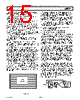
18 / 23 page  REV. PrA PRELIMINARY TECHNICAL DATA –18– AD7667 t1 t3 t4 t11 CNVST BUSY DATA BUS CS = RD = 0 t10 PREVIOUS CONVERSION DATA NEW DATA Figure 13. Master Parallel Data Timing for Reading (Continuous Read) PARALLEL INTERFACE The AD7667 is configured to use the parallel interface when the SER/ PAR is held low. The data can be read either after each conversion, which is during the next acquisition phase, or during the following conversion as shown, respectively, in Figure 14 and Figure 15. When the data is read during the conversion, however, it is recommended that it is read only during the first half of the conversion phase. That avoids any potential feedthrough between voltage transients on the digital interface and the most critical analog conversion cir- cuitry. CURRENT CONVERSION BUSY DATA BUS CS RD t12 t13 Figure 14. Slave Parallel Data Timing for Reading (Read After Convert) The BYTESWAP pin allows a glueless interface to a 8 bits bus. As shown in Figure TBD, the LSB byte is output on D[7:0] and the MSB is output on D[15:8] when BYTESWAP is low. When BYTESWAP is high, the LSB and MSB bytes are swapped and the LSB is output on D[15:8] and the MSB is output on D[7:0]. By connecting BYTESWAP to an address line, the 16 bits data can be read in 2 bytes on either D[15:8] or D[7:0]. SCLK SDOUT D15 D14 D1 D0 D13 X15 X14 X13 X1 X0 Y15 Y14 CS BUSY SDIN EXT/INT = 1 INVSCLK = 0 t35 t36 t37 t31 t32 t16 t33 t34 X15 X14 X 1 2 3 1415 1617 18 RD = 0 Figure 18. Slave Serial Data Timing for Reading (Read After Convert) |
|
|
Link URL |
| Does ALLDATASHEET help your business so far? [ DONATE ] |
About Alldatasheet | Advertisement | Contact us | Privacy Policy | Link to Datasheet | Link Exchange | Manufacturer List All Rights Reserved©Alldatasheet.com |
| Russian : Alldatasheetru.com | Korean : Alldatasheet.co.kr | Spanish : Alldatasheet.es | French : Alldatasheet.fr | Italian : Alldatasheetit.com Portuguese : Alldatasheetpt.com | Polish : Alldatasheet.pl | Vietnamese : Alldatasheet.vn Indian : Alldatasheet.in | Mexican : Alldatasheet.com.mx | British : Alldatasheet.co.uk | New Zealand : Alldatasheet.co.nz |
|
Family Site : ic2ic.com |
icmetro.com |
 English ▼
 English
 Chinese
 German
 Japanese
 Russian
 Korean
 Spanish
 French
 Italian
 Portuguese
 Polish
 Vietnamese
 Indian
 Mexican
 British
 New Zealand