|
Electronic Components Datasheet Search |
|
|
Electronic Components Datasheet Search |
|
LTC1540CS8 Datasheet(PDF) 7 Page - Linear Technology |
|
|
|||||||||||||||||||||||||||||
LTC1540CS8 Datasheet(HTML) 7 Page - Linear Technology |
|
|
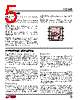
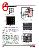
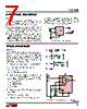
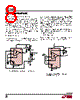
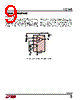
7 / 12 page  7 LTC1540 sn1540 1540fas APPLICATIONS INFORMATION Hysteresis Hysteresis can be added to the LTC1540 by connecting a resistor (R1) between the REF and HYST pins and a second resistor (R2) from HYST to V – (Figure 5). The difference between the upper and lower threshold voltages, or hysteresis voltage band (VHB), is equal to twice the voltage difference between the REF and HYST pins. When more hysteresis is added, the upper threshold increases the same amount as the low threshold de- creases. The maximum voltage allowed between REF and HYST pins is 50mV, producing a maximum hysteresis voltage band of 100mV. The hysteresis band may vary by up to 15%. If hysteresis is not wanted, the HYST pin should be shorted to REF. Acceptable values for IREF range from 0.1µA to 5µA. If 2.4M is chosen for R2, then the value of R1 (kΩ) is equal to the value of VHB (mV). 6 R2 HYST V– REF 5 R1 1540 • F05 LTC1540 2 IREF R1 = VHB (2)(IREF) R2 = IREF 1.182V – () VHB 2 Figure 5. Programmable Hysteresis Figure 6. Glitch-Free Level Detector with Hysteresis TYPICAL APPLICATIONS Level Detector The LTC1540 is ideal for use as a nanopower level detector as shown in Figure 6. R1 and R2 form a voltage divider from VIN to the noninverting comparator input. R3 and R4 set the hysteresis voltage, and R5 and C1 bypass the reference output. The following design procedure can be used to select the component values: 1. Choose the VIN voltage trip level, in this example 4.65V. 2. Calculate the required resistive divider ratio. Ratio = VREF/VIN Ratio = 1.182V/4.65V = 0.254 3. Choose the required hysteresis voltage band at the input VHBIN, in this example 60mV. Calculate the hyster- esis voltage band referred to the comparator input VHB. VHB = (VHBIN)(Ratio) VHB = (60mV)(0.254) VHB = 15.24mV 4. Choose the values for R3 and R4 to set the hysteresis. R4 = 2.4M R3 (kΩ) = 15k, VHB (mV) = 15mV 5. Choose the values for R1 and R2 to set the trip point. R1 = R2 = R1 – 1 = = 1.18M VREF IBIAS VREF + VIN VHB 2 1.182V 1µA R2 = 1.18M R2 = 3.40M – 1 1.182V + 4.65V 15mV 2 V + R5 430Ω 5% R3 15k 1% C1 1µF OUT V – 21 7 5V VIN 8 GND LTC1540 1540 F06 IN+ IN– HYST REF 3 4 5 6 – + R2 3.4M 1% R1 1.18M 1% R4 2.4M 1% |
|
|
Link URL |
| Does ALLDATASHEET help your business so far? [ DONATE ] |
About Alldatasheet | Advertisement | Contact us | Privacy Policy | Link to Datasheet | Link Exchange | Manufacturer List All Rights Reserved©Alldatasheet.com |
| Russian : Alldatasheetru.com | Korean : Alldatasheet.co.kr | Spanish : Alldatasheet.es | French : Alldatasheet.fr | Italian : Alldatasheetit.com Portuguese : Alldatasheetpt.com | Polish : Alldatasheet.pl | Vietnamese : Alldatasheet.vn Indian : Alldatasheet.in | Mexican : Alldatasheet.com.mx | British : Alldatasheet.co.uk | New Zealand : Alldatasheet.co.nz |
|
Family Site : ic2ic.com |
icmetro.com |
 English ▼
 English
 Chinese
 German
 Japanese
 Russian
 Korean
 Spanish
 French
 Italian
 Portuguese
 Polish
 Vietnamese
 Indian
 Mexican
 British
 New Zealand