|
Electronic Components Datasheet Search |
|
|
Electronic Components Datasheet Search |
|
LTC1540CS8 Datasheet(PDF) 6 Page - Linear Technology |
|
|
|||||||||||||||||||||||||||||
LTC1540CS8 Datasheet(HTML) 6 Page - Linear Technology |
|
|
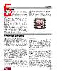
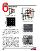
6 / 12 page  6 LTC1540 sn1540 1540fas APPLICATIONS INFORMATION V + R1 430Ω R2 10k C1 1µF 5V TO 8V OUT V – 21 7 8 GND LTC1540 1540 • F03a IN+ IN– HYST REF 3 4 5 6 R3 2.4M – + LTC1540 V – REF R1 C1 REFERENCE OUTPUT 1540 • F01 Figure 1. Damping the Reference Output Figure 2. Damping Resistance vs Bypass Capacitor Value Figure 3 shows the bypassed reference output with a square wave applied to the V + pin. Resistors R2 and R3 set 10mV of hysteresis voltage band while R1 damps the reference response. Note that the comparator output doesn’t trip. Low Voltage Operation: V + = 1.6V The guaranteed minimum operating voltage is 2V (or ±1V). As the total supply voltage is reduced below 2V, the performance degrades and the supply current falls. At low supply voltages, the comparator’s output drive is reduced and the propagation delay increases. The VREF and VOS are also slightly worse. The useful input voltage range extends from the negative supply to 0.9V below the positive supply. Test your prototype over the full temperature and supply voltage range if operation below 2V is anticipated. Because of the increase in supply current, operation below 1.5V is not recommended (Figure 4). Figure 4. Supply Current vs Supply Voltage SUPPLY VOLTAGE (V) 0 3 4 5 2.0 1540 F04 2 1 0 0.5 1.0 1.5 2.5 V – = GND = 0V IN+ = 0V IN– = REF = HYST TA = 25°C Figure 3a. Power Supply Transient Test Circuit CAPACITOR VALUE (µF) 0.001 0.1 10 1000 0.01 0.1 10 1 1540 • F02 1 100 Figure 3b. Power Supply Transient Rejection 2ms/DIV 1540 F03b 8V V + 5V VREF OUT |
|
|
Link URL |
| Does ALLDATASHEET help your business so far? [ DONATE ] |
About Alldatasheet | Advertisement | Contact us | Privacy Policy | Link to Datasheet | Link Exchange | Manufacturer List All Rights Reserved©Alldatasheet.com |
| Russian : Alldatasheetru.com | Korean : Alldatasheet.co.kr | Spanish : Alldatasheet.es | French : Alldatasheet.fr | Italian : Alldatasheetit.com Portuguese : Alldatasheetpt.com | Polish : Alldatasheet.pl | Vietnamese : Alldatasheet.vn Indian : Alldatasheet.in | Mexican : Alldatasheet.com.mx | British : Alldatasheet.co.uk | New Zealand : Alldatasheet.co.nz |
|
Family Site : ic2ic.com |
icmetro.com |
 English ▼
 English
 Chinese
 German
 Japanese
 Russian
 Korean
 Spanish
 French
 Italian
 Portuguese
 Polish
 Vietnamese
 Indian
 Mexican
 British
 New Zealand