|
Electronic Components Datasheet Search |
|
|
Electronic Components Datasheet Search |
|
MAX5259EEE Datasheet(PDF) 10 Page - Maxim Integrated Products |
|
|
|||||||||||||||||||||||||||||
MAX5259EEE Datasheet(HTML) 10 Page - Maxim Integrated Products |
|
|
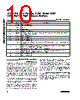
10 / 20 page  +3V/+5V, Low-Power, 8-Bit Octal DAC with Rail-to-Rail Output Buffers 10 ______________________________________________________________________________________ Detailed Description Serial Interface At power-on, the serial interface and all DACs are cleared and set to code zero. The serial data output (DOUT) is set to transition on SCLK’s falling edge. The MAX5258/MAX5259 communicate with micro- processors (µPs) through a synchronous, 3-wire inter- face (Figure 1). Data is sent MSB first and can be transmitted in two 4-bit and one 8-bit (byte) packets, or one 16-bit word. The first two bits are ignored. A 4-wire interface adds a line for LDAC, allowing asynchronous updating. Data is transmitted and received simultane- ously. Figure 2 shows the detailed serial-interface timing. Note that the clock should be low if it is stopped between updates. DOUT does not go into a high-impedance state if the clock idles or CS is high. Serial data is clocked into the data registers in MSB-first format, with the address and configuration information preceding the actual DAC data. Data is clocked in on SCLK’s rising edge while CS is low. Data at DOUT is clocked out 16 clock cycles later, either at SCLK’s falling edge (default or mode 0) or rising edge (mode 1). CS must be low to enable the device. If CS is high, the interface is disabled and DOUT remains unchanged. CS must go low at least 40ns before the first rising edge of the clock pulse to properly clock in the first bit. With CS low, data is clocked into the MAX5258/MAX5259’s internal shift register on the rising edge of the external serial clock. Always clock in the full 16 bits. Serial Input Data Format and Control Codes The 16-bit serial input format, shown in Figure 3, com- prises two “don’t care” bits, three DAC address bits (A2, A1, A0), three control bits (C2, C1, C0), and eight data bits (D7…D0). The 6-bit address/control code configures the DAC as shown in Table 1. Pin Description PIN NAME FUNCTION 1 OUTB DAC B Voltage Output 2 OUTA DAC A Voltage Output 3 GND Ground 4VDD Power Supply 5 REF Reference Voltage Input 6 LDAC Load DAC Input. Driving this asynchronous input low transfers the contents of each input register to its respective DAC registers. 7 OUTE DAC E Voltage Output 8 OUTF DAC F Voltage Output 9 OUTG DAC G Voltage Output 10 OUTH DAC H Voltage Output 11 CS Chip Select Input. Data is shifted in and out when CS is low. Programming commands are executed when CS returns high. 12 SCLK Serial Clock Input. Data is clocked in on the rising edge and clocked out on the falling edge (default) or rising edge (A2 = 1; see Table 1). 13 DIN Serial Data Input. Data is clocked in on the rising edge of SCLK. 14 DOUT Serial Data Output. Sinks and sources current. Data at DOUT can be clocked out on the falling edge (mode 0) or rising edge (mode 1) of SCLK (Table 1). 15 OUTD DAC D Voltage Output 16 OUTC DAC C Voltage Output |
|
|
Link URL |
| Does ALLDATASHEET help your business so far? [ DONATE ] |
About Alldatasheet | Advertisement | Contact us | Privacy Policy | Link to Datasheet | Link Exchange | Manufacturer List All Rights Reserved©Alldatasheet.com |
| Russian : Alldatasheetru.com | Korean : Alldatasheet.co.kr | Spanish : Alldatasheet.es | French : Alldatasheet.fr | Italian : Alldatasheetit.com Portuguese : Alldatasheetpt.com | Polish : Alldatasheet.pl | Vietnamese : Alldatasheet.vn Indian : Alldatasheet.in | Mexican : Alldatasheet.com.mx | British : Alldatasheet.co.uk | New Zealand : Alldatasheet.co.nz |
|
Family Site : ic2ic.com |
icmetro.com |
 English ▼
 English
 Chinese
 German
 Japanese
 Russian
 Korean
 Spanish
 French
 Italian
 Portuguese
 Polish
 Vietnamese
 Indian
 Mexican
 British
 New Zealand