|
Electronic Components Datasheet Search |
|
|
Electronic Components Datasheet Search |
|
TLE7209-2R Datasheet(PDF) 10 Page - Infineon Technologies AG |
|
|
|||||||||||||||||||||||||||||
TLE7209-2R Datasheet(HTML) 10 Page - Infineon Technologies AG |
|
|
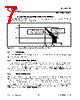
10 / 32 page  TLE 7209-2R Circuit Description Preliminary Datasheet 10 V1.0, 2004-mar-12 The first two bits of an instruction may be used to establish an extended device- addressing. This gives the opportunity to operate up to 4 Slave-devices sharing one common CSN signal from the Master-Unit (see Figure 7) Figure 6 SPI block-diagram 2.4.2.2 Characteristics of the SPI Interface 1. When DMS is > 3.5V, the SPI is active, independently of the state of EN or DIS. During active reset conditions (DMS < 3.5V) the SPI is driven into its default state. When reset becomes inactive, the state machine enters into a wait-state for the next instruction. 2. If the slave select signal at CSN is inactive (high), the state machine is forced to enter the wait-state, i.e. the state machine waits for the following instruction. 3. During active (low) state of the select signal CSN the falling edge of the serial clock signal SCK will be used to latch the input data at SDI. Output data at SDO are driven with the rising edge of SCK (see timing diagram Figure 13) 4. Chip-address: In order to establish the option of extended addressing the uppermost two bits of the instruction-byte (i.e the first two SDI-bits of a Frame) are reserved to send a chip- address. To avoid a bus conflict the output SDO must stay high impedance during the addressing phase of a frame (i.e. until the address-bits are recognized as valid chip- address). If the chip-address does not match, the data at SDI will be ignored and SDO remains high impedance for the complete frame. See also Figure 7 5. Verification byte: Simultaneously to the receipt of an SPI instruction TLE 7209-2R transmits a verification byte via the output SDO to the controller. Refer to Figure 8. This byte indicates normal or abnormal operation of the SPI. It contains an initial bit pattern and a flag indicating an error occurred during the previous access. CS N DM S SC K SD I SD O s h ift- r e gis t er S P I- C on t r ol: - > s tate m a c h in e - > clo c k c o u n te r - > in str u ctio n r e co g n itio n S P I pow er - su p p ly DIA _ RE G D ia gno s tic s 8 8 OR EN DIS Re s e t DM S U nde r - vo lta g e |
|
Link URL |
| Does ALLDATASHEET help your business so far? [ DONATE ] |
About Alldatasheet | Advertisement | Contact us | Privacy Policy | Link to Datasheet | Link Exchange | Manufacturer List All Rights Reserved©Alldatasheet.com |
| Russian : Alldatasheetru.com | Korean : Alldatasheet.co.kr | Spanish : Alldatasheet.es | French : Alldatasheet.fr | Italian : Alldatasheetit.com Portuguese : Alldatasheetpt.com | Polish : Alldatasheet.pl | Vietnamese : Alldatasheet.vn Indian : Alldatasheet.in | Mexican : Alldatasheet.com.mx | British : Alldatasheet.co.uk | New Zealand : Alldatasheet.co.nz |
|
Family Site : ic2ic.com |
icmetro.com |
 English ▼
 English
 Chinese
 German
 Japanese
 Russian
 Korean
 Spanish
 French
 Italian
 Portuguese
 Polish
 Vietnamese
 Indian
 Mexican
 British
 New Zealand