|
Electronic Components Datasheet Search |
|
|
Electronic Components Datasheet Search |
|
ADN8102ACPZ-R7 Datasheet(PDF) 21 Page - Analog Devices |
|
|
|||||||||||||||||||||||||||||
ADN8102ACPZ-R7 Datasheet(HTML) 21 Page - Analog Devices |
|
|
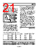
21 / 36 page  ADN8102 Rev. C | Page 21 of 36 TRANSMITTERS Output Structure and Output Levels The ADN8102 transmitter outputs incorporate 50 Ω termina- tion resistors, ESD protection, and an output current switch. Each port provides control of both the absolute output level and the pre-emphasis output level. It should be noted that the choice of output level affects the output common-mode level. A 600 mV peak-to-peak differential output level with full pre-emphasis range requires an output termination voltage of 2.5 V or greater (VTTO, VCC ≥ 2.5 V). VCC VTTO OP ON VEE Tx SIMPLIFIED DIAGRAM Q1 Q2 ITOT RN 50Ω RP 50Ω ON-CHIP TERMINATION V3 VC V2 VP V1 VN IDC + IPE ESD Figure 41. Simplified Output Structure Pre-Emphasis The total output amplitude and pre-emphasis setting space is reduced to a single map of basic settings that provide seven settings of output equalization to ease programming for typical channels. The PE_A/PE_B[1:0] pins provide selections 0, 2, 4, and 6 of the seven pre-emphasis settings through toggle pin control, covering the entire range of settings at lower resolution. The full resolution of seven settings is available through the I2C interface by writing to Bits[2:0] (PE[2:0] of the OUT_A/OUT_B configuration registers) with I2C settings overriding the toggle pin control. Similar to the receiver settings, the ADN8102 allows joint control of all four channels in a transmit port. Table 15 summarizes the absolute output level, pre-emphasis level, and high frequency boost for each of the basic control settings and the typical length of the CX4 cable and FR4 trace that each setting compensates. Full control of the transmit output levels is available through the I2C control interface. This full control is achieved by writing to the OUT_A/OUT_B Output Level Control[1:0] registers for the channel of interest. Table 17 shows the supported output level settings of the OUT_A/OUT_B Output Level Control[1:0] registers. Register settings not listed in Table 17 are not supported by the ADN8102. The output equalization is optimized for less than 1.75 Gbps operation but can be optimized for higher speed applications at up to 3.75 Gbps through the I2C control interface by writing to the DATA RATE bit (Bit 4) of the OUT_A/OUT_B configuration registers, with high representing 3.75 Gbps and low representing 1.75 Gbps. The PE CTL SRC bit (Bit 7) in the OUT_A/OUT_B Output Level Control 1 register determines whether the pre- emphasis and output current controls for the channel of interest are selected from the optimized map or directly from the OUT_A/ OUT_B Output Level Control[1:0] registers (per channel). Setting this bit high selects pre-emphasis control directly from the OUT_A/OUT_B Output Level Control[1:0] registers, and setting it low selects pre-emphasis control from the optimized map. Table 14. Data Rate Select OUT_A/OUT_B Configuration Bit 4 Supported Data Rates 0 (default) 0 Gbps to 1.75 Gbps 1 1.75 Gbps to 3.75 Gbps Table 15. Transmit Pre-Emphasis Boost and Overshoot vs. Setting PE[2:0] Register PE[1:0] Pins Boost (dB) Overshoot (%) DC Swing (mV p-p diff) Typical CX4 Cable Length (Meters) Typical FR4 Trace Length (Inches) 0 0 0 0 800 0 to 2.5 0 to 5 1 Not applicable 2 25 800 2.5 to 5 0 to 5 2 1 3.5 50 800 5 to 7.5 10 to 15 3 Not applicable 4.9 75 800 7.5 to 10 10 to 15 4 2 6 100 800 10 to 12.5 15 to 20 5 Not applicable 7.4 133 600 15 to 17.5 20 to 25 6 4 9.5 200 400 20 to 22.5 25 to 30 Table 16. Output Configuration Registers Name Address Bit 7 Bit 6 Bit 5 Bit 4 Bit 3 Bit 2 Bit 1 Bit 0 Default OUT_A/OUT_B configuration 0xC0, 0xE0 EN DATA RATE PE[2] PE[1] PE[0] 0x20 OUT_A/OUT_B Output Level Control 1 0xC1, 0xE1 PE CTL SRC OUTx_OLEV1[6:0] 0x40 OUT_A/OUT_B Output Level Control 0 0xC2, 0xE2 OUTx_OLEV0[6:0] 0x40 |
|
Link URL |
| Does ALLDATASHEET help your business so far? [ DONATE ] |
About Alldatasheet | Advertisement | Contact us | Privacy Policy | Link to Datasheet | Link Exchange | Manufacturer List All Rights Reserved©Alldatasheet.com |
| Russian : Alldatasheetru.com | Korean : Alldatasheet.co.kr | Spanish : Alldatasheet.es | French : Alldatasheet.fr | Italian : Alldatasheetit.com Portuguese : Alldatasheetpt.com | Polish : Alldatasheet.pl | Vietnamese : Alldatasheet.vn Indian : Alldatasheet.in | Mexican : Alldatasheet.com.mx | British : Alldatasheet.co.uk | New Zealand : Alldatasheet.co.nz |
|
Family Site : ic2ic.com |
icmetro.com |
 English ▼
 English
 Chinese
 German
 Japanese
 Russian
 Korean
 Spanish
 French
 Italian
 Portuguese
 Polish
 Vietnamese
 Indian
 Mexican
 British
 New Zealand