|
Electronic Components Datasheet Search |
|
|
Electronic Components Datasheet Search |
|
STM32U545NET3QTR Datasheet(PDF) 212 Page - STMicroelectronics |
|
|
|||||||||||||||||||||||||||||
STM32U545NET3QTR Datasheet(HTML) 212 Page - STMicroelectronics |
|
|
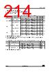
212 / 283 page  Electrical characteristics STM32U545xx 212/283 DS14216 Rev 1 11 (cont’d) tr/tf Output rise and fall time FT_v and TT_v I/Os CL = 30 pF, 2.7 V ≤ VDDIOx ≤ 3.6 V - 2.5(5) ns CL = 30 pF, 1.58 V ≤ VDDIOx < 2.7 V - 5.0(5) CL = 30 pF, 1.08 V ≤ VDDIOx < 1.58 V - 11 CL = 10 pF, 2.7 V ≤ VDDIOx ≤ 3.6 V - 1.66(5) CL = 10 pF, 1.58 V ≤ VDDIOx < 2.7 V - 3.1(5) CL = 10 pF, 1.08 V ≤ VDDIOx < 1.58 V - 7 Fm+ Fmax Maximum frequency CL = 550 pF, 1.08 V ≤ VDDIOx < 3.6 V - 1 MHz tf Output fall time(6) CL = 100 pF, 1.58 V ≤ VDDIOx < 3.6 V - 50 ns CL = 100 pF, 1.08 V ≤ VDDIOx < 1.58 V - 80 CL = 550 pF, 1.58 V ≤ VDDIOx < 3.6 V - 100 CL = 550 pF, 1.08 V ≤ VDDIOx < 1.58 V - 220 1. FT_t I/O characteristics are degraded only in VBAT mode (refer to Table 99). 2. The I/O structure options listed in this table can be a concatenation of options including the option explicitly listed. For instance TT_a refers to any TT I/O with _a option. TT_xx refers to any TT I/O and FT_xx refers to any FT I/O. 3. The I/O speed is configured using the OSPEEDRy[1:0] bits. Refer to the product reference manual for a description of GPIO port configuration register. 4. Specified by design. Not tested in production. 5. Compensation system enabled. 6. The fall time is defined between 70% and 30% of the output waveform accordingly to I2C specification. Table 96. Output AC characteristics, HSLV OFF (all I/Os except FT_c, FT_t in VBAT mode, and FT_o I/Os(1))(2)(3)(4) (continued) Speed Symbol Parameter Conditions Min Max Unit Table 97. Output AC characteristics, HSLV ON (all I/Os except FT_c)(1)(2)(3)(4) Speed Symbol Parameter Conditions Min Max Unit 00 Fmax Maximum frequency CL = 50 pF, 1.58 V ≤ VDDIOx < 2.7 V - 10 MHz CL = 50 pF, 1.08 V ≤ VDDIOx < 1.58 V - 4 CL = 10 pF, 1.58 V ≤ VDDIOx < 2.7 V - 15 CL = 10 pF, 1.08 V ≤ VDDIOx < 1.58 V - 4 tr/tf Output rise and fall time CL = 50 pF, 1.58 V ≤ VDDIOx < 2.7 V - 18 ns CL = 50 pF, 1.08 V ≤ VDDIOx < 1.58 V - 32 CL = 10 pF, 1.58 V ≤ VDDIOx < 2.7 V - 12 CL = 10 pF, 1.08 V ≤ VDDIOx < 1.58 V - 21 |
|
Link URL |
| Does ALLDATASHEET help your business so far? [ DONATE ] |
About Alldatasheet | Advertisement | Contact us | Privacy Policy | Link to Datasheet | Link Exchange | Manufacturer List All Rights Reserved©Alldatasheet.com |
| Russian : Alldatasheetru.com | Korean : Alldatasheet.co.kr | Spanish : Alldatasheet.es | French : Alldatasheet.fr | Italian : Alldatasheetit.com Portuguese : Alldatasheetpt.com | Polish : Alldatasheet.pl | Vietnamese : Alldatasheet.vn Indian : Alldatasheet.in | Mexican : Alldatasheet.com.mx | British : Alldatasheet.co.uk | New Zealand : Alldatasheet.co.nz |
|
Family Site : ic2ic.com |
icmetro.com |
 English ▼
 English
 Chinese
 German
 Japanese
 Russian
 Korean
 Spanish
 French
 Italian
 Portuguese
 Polish
 Vietnamese
 Indian
 Mexican
 British
 New Zealand