|
Electronic Components Datasheet Search |
|
|
Electronic Components Datasheet Search |
|
AM29BDS643G Datasheet(PDF) 45 Page - Advanced Micro Devices |
|
|
|||||||||||||||||||||||||||||
AM29BDS643G Datasheet(HTML) 45 Page - Advanced Micro Devices |
|
|
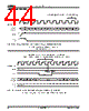
45 / 49 page  May 8, 2006 25692A2 Am29BDS643G 43 D A TA SH EE T AC CHARACTERISTICS Note: Devices should be programmed with wait states as discussed in the “Programmable Wait State” section on page 10. Figure 20. Initial Access with Power Saving (PS) Function and Address Boundary Latency Note: If tAVDSM > 1 CLK cycle, wait state usage is reduced. Figure shows 40 MHz clock, handshaking enabled. Wait state usage is 4 clock cycles instead of 5. Note that tAVDSM must be less than 76 µs for burst operation to begin. Figure 21. Example of Extended Valid Address Reducing Wait State Usage CLK AVD# RDY PS Address High-Z High-Z A/DQ0: A/DQ15 PS OE# D0 D1 D2 PS1 PS2 device is programmable from 2 to 7 total cycles during initial access (here, programmable wait state function is set to 04h; 6 cycles total) PS high if data is inverted, low if data is not inverted 2 additional wait states if address is at boundary 1 additional wait state to indicate PS is enabled AVD# low with clock present enables burst read mode Address A16:A21 boundary latency tOE CLK AVD# RDY High-Z A/DQ OE# CE# D0 D1 D2 tIACC2 tAVDSM Addresses |
|
Link URL |
| Does ALLDATASHEET help your business so far? [ DONATE ] |
About Alldatasheet | Advertisement | Contact us | Privacy Policy | Link to Datasheet | Link Exchange | Manufacturer List All Rights Reserved©Alldatasheet.com |
| Russian : Alldatasheetru.com | Korean : Alldatasheet.co.kr | Spanish : Alldatasheet.es | French : Alldatasheet.fr | Italian : Alldatasheetit.com Portuguese : Alldatasheetpt.com | Polish : Alldatasheet.pl | Vietnamese : Alldatasheet.vn Indian : Alldatasheet.in | Mexican : Alldatasheet.com.mx | British : Alldatasheet.co.uk | New Zealand : Alldatasheet.co.nz |
|
Family Site : ic2ic.com |
icmetro.com |
 English ▼
 English
 Chinese
 German
 Japanese
 Russian
 Korean
 Spanish
 French
 Italian
 Portuguese
 Polish
 Vietnamese
 Indian
 Mexican
 British
 New Zealand