|
Electronic Components Datasheet Search |
|
|
Electronic Components Datasheet Search |
|
LT8418ACBZ-R7 Datasheet(PDF) 1 Page - Analog Devices |
|
|
|||||||||||||||||||||||||||||
LT8418ACBZ-R7 Datasheet(HTML) 1 Page - Analog Devices |
|
|
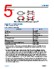
1 / 19 page  Data Sheet LT8418 100V Half-Bridge GaN Driver with Smart Integrated Bootstrap Switch Pre-release Rev 0 DOCUMENT FEEDBACK TECHNICAL SUPPORT One Analog Wa y, Wilmington, MA 01887 -2356, U.S.A. Tel: 781.329.47 00 ©2023 Analog Devices, Inc. Al l rights rese rve d. FEATURES Half-Bridge Gate Driver for GaN FETs 0.6Ω Pull-Up Resistance at Top Gate Driver 0.2Ω Pull-Down Resistance at Bottom Gate Driver 4A Peak Source, 8A Peak Sink Current Capability Smart Integrated Bootstrap Switch Split-Gate-Driver to Adjust Turn-On/Turn-Off Strength Default Low-State for All Driver Inputs and Outputs Maximum 15V Voltage Rating at INT and INB Inputs Independent INT, INB Inputs with TTL Logic Compatible Fast Propagation Delay: 10ns (Typical) Propagation Delay Matching: 1.5ns (Typical) Balanced Driver Supply Voltage: VBST ≈ VCC = 3.85V – 5.5V Undervoltage and Overvoltage Lockout Protections Small 12-Ball WLCSP Package APPLICATIONS High Frequency DC-DC Switching Power Converters Half-Bridge, Full-Bridge, Push-Pull Converters Data Center Power Supplies Motor Drivers, Class-D Audio Amplifiers Consumer, Industrial, and Automotive GENERAL DESCRIPTION The LT8418 is a 100V half-bridge GaN driver that integrates top and bottom driver stages, driver logic control, and protections. It can be configured into synchronous half-bridge, full-bridge topologies, or buck, boost, and buck-boost topologies. The LT8418 provides strong current sourcing/sinking capability with 0.6Ω pull-up and 0.2Ω pull-down resistance. It also integrates smart integrated bootstrap switch to generate a balanced bootstrap voltage from VCC with a minimum dropout voltage. The LT8418 provides split gate drivers to adjust the turn- on and turn-off slew rates of GaN FETs to suppress ringing and optimize EMI performance. All driver inputs and outputs have default low-state to prevent GaN FETs from false turn-on. The inputs of the LT8418, INT, and INB are independent and TTL logic compatible. Meanwhile, the LT8418 performs with a fast propagation delay of 10ns and maintains an excellent delay matching of 1.5ns between the top and bottom channels, making it suitable for high-frequency DC-DC converters, motor drivers, and class-D audio amplifiers. In addition, the LT8418 employs the WLCSP package to minimize parasitic inductance, enabling its wide use in high- performance and high-power density applications. TYPICAL APPLICATION Figure 1. Highly Efficient GaN-Based Switching DC-DC Converter 0.1µF 4.7µF 10µF GaN FET GaN FET 10µH 3.3Ω 3.3Ω 0.1µF 10µF BST TGP TGN SW BGP BGN GND VCC INB INT VCC SW TOP SIDE INPUT: INT BOTTOM SIDE INPUT: INB VIN 100V MAX VCC 3.85V TO 5.5V VOUT 100V MAX LT8418 |
Similar Part No. - LT8418ACBZ-R7 |
|
Similar Description - LT8418ACBZ-R7 |
|
|
|
Link URL |
| Does ALLDATASHEET help your business so far? [ DONATE ] |
About Alldatasheet | Advertisement | Contact us | Privacy Policy | Link to Datasheet | Link Exchange | Manufacturer List All Rights Reserved©Alldatasheet.com |
| Russian : Alldatasheetru.com | Korean : Alldatasheet.co.kr | Spanish : Alldatasheet.es | French : Alldatasheet.fr | Italian : Alldatasheetit.com Portuguese : Alldatasheetpt.com | Polish : Alldatasheet.pl | Vietnamese : Alldatasheet.vn Indian : Alldatasheet.in | Mexican : Alldatasheet.com.mx | British : Alldatasheet.co.uk | New Zealand : Alldatasheet.co.nz |
|
Family Site : ic2ic.com |
icmetro.com |
 English ▼
 English
 Chinese
 German
 Japanese
 Russian
 Korean
 Spanish
 French
 Italian
 Portuguese
 Polish
 Vietnamese
 Indian
 Mexican
 British
 New Zealand