|
Electronic Components Datasheet Search |
|
|
Electronic Components Datasheet Search |
|
SA2159 Datasheet(PDF) 8 Page - Silan Microelectronics Joint-stock |
|
|
|||||||||||||||||||||||||||||
SA2159 Datasheet(HTML) 8 Page - Silan Microelectronics Joint-stock |
|
|
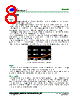
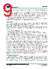
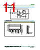
8 / 11 page  SA2159 HANGZHOU SILAN MICROELECTRONICS CO.,LTD Rev: 1.0 2005.04.22 Http: www.silan.com.cn Page 8 of 11 APPLICATIONS Input As mentioned above, because input and output signals are currents, not voltages, the current input/output mode provides great flexibility in application. Internal negative feedback loop provides a virtual ground to the input pin 1 (See Figure 1). Within the linear range of the device, the input resistor (shown as 20k Ω in typical application circuit) should be scaled to convert the available ac input voltage to a current. In order to obtain best distortion performance, peak input currents should be kept under 1 mA. The input impedances must be less than 30k Ω to assure the circuit stability. The feedback impedances around the internal op amp (essentially Q1/D1 and Q3/D3) are fixed. Low values for the input resistor will require more closed-loop gain from the op amp. Since the open-loop gain naturally falls off at high frequencies, this resistor should be kept to 10k Ω or above in order to prevent high frequency distortion when the gain is too much. Distortion vs. frequency for a 1V signal at 0dB gain with a 20 k Ω input resistor is shown in Figure 9. As mentioned above, any dc input currents will cause dc signals in the output. The dc signals will be modulated by gain command, in turn causing audible thump. Therefore, in order to control quality audio applications, capacitive coupling must be adopted in actual application, which can give acceptable low frequency performance. Figure 9. Typical THD Vs. frequency, 0dB gain Output The output pin (pin 8) should be connected to a virtual ground node, so that current flowing in it may be converted to a voltage. Choose the external op amp can improve audio performance. A small feedback capacitor around the output op amp is necessary to cancel the output capacitance of the VCA, so that most op amps can operate steadily. The capacitance at pin 8 is typically 30 pf. Power supplies The positive supply is connected directly to pin 7 without special bypassing circuit, but it is good practice to include a small (~1 µf) electrolytic close to the VCA IC on the PCB. There is no particularly dependence between performance and supply voltage. The lowest supply voltage is determined by the sum of the input and output currents plus ISET, which must be supplied through the resistor (~2k Ω) at the top of the core transistors while still allowing enough voltage swing to bias the internal op amp and the core transistors themselves. Reducing signal currents may help accommodate low supply voltages. |
|
|
Link URL |
| Does ALLDATASHEET help your business so far? [ DONATE ] |
About Alldatasheet | Advertisement | Contact us | Privacy Policy | Link to Datasheet | Link Exchange | Manufacturer List All Rights Reserved©Alldatasheet.com |
| Russian : Alldatasheetru.com | Korean : Alldatasheet.co.kr | Spanish : Alldatasheet.es | French : Alldatasheet.fr | Italian : Alldatasheetit.com Portuguese : Alldatasheetpt.com | Polish : Alldatasheet.pl | Vietnamese : Alldatasheet.vn Indian : Alldatasheet.in | Mexican : Alldatasheet.com.mx | British : Alldatasheet.co.uk | New Zealand : Alldatasheet.co.nz |
|
Family Site : ic2ic.com |
icmetro.com |
 English ▼
 English
 Chinese
 German
 Japanese
 Russian
 Korean
 Spanish
 French
 Italian
 Portuguese
 Polish
 Vietnamese
 Indian
 Mexican
 British
 New Zealand