|
Electronic Components Datasheet Search |
|
|
Electronic Components Datasheet Search |
|
CC1100-RTY1 Datasheet(PDF) 29 Page - Texas Instruments |
|
|
|
|||||||||||||||||||||||||||||
CC1100-RTY1 Datasheet(HTML) 29 Page - Texas Instruments |
|
|
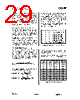
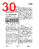
29 / 100 page  CC1100 SWRS038D Page 29 of 92 With default PTEST register setting (0x7F) the temperature sensor output is only available when the frequency synthesizer is enabled (e.g. the MANCAL, FSTXON, RX, and TX states). It is necessary to write 0xBF to the PTEST register to use the analog temperature sensor in the IDLE state. Before leaving the IDLE state, the PTEST register should be restored to its default value (0x7F). 11.3 Optional Radio Control Feature The CC1100 has an optional way of controlling the radio, by reusing SI, SCLK, and CSn from the SPI interface. This feature allows for a simple three-pin control of the major states of the radio: SLEEP, IDLE, RX, and TX. This optional functionality is enabled with the MCSM0.PIN_CTRL_EN configuration bit. State changes are commanded as follows: When CSn is high the SI and SCLK is set to the desired state according to Table 18. When CSn goes low the state of SI and SCLK is latched and a command strobe is generated internally according to the pin configuration. It is only possible to change state with this functionality. That means that for instance RX will not be restarted if SI and SCLK are set to RX and CSn toggles. When CSn is low the SI and SCLK has normal SPI functionality. All pin control command strobes are executed immediately, except the SPWD strobe, which is delayed until CSn goes high. CSn SCLK SI Function 1 X X Chip unaffected by SCLK/SI ↓ 0 0 Generates SPWD strobe ↓ 0 1 Generates STX strobe ↓ 1 0 Generates SIDLE strobe ↓ 1 1 Generates SRX strobe 0 SPI mode SPI mode SPI mode (wakes up into IDLE if in SLEEP/XOFF) Table 18: Optional Pin Control Coding 12 Data Rate Programming The data rate used when transmitting, or the data rate expected in receive is programmed by the MDMCFG3.DRATE_M and the MDMCFG4.DRATE_E configuration registers. The data rate is given by the formula below. As the formula shows, the programmed data rate depends on the crystal frequency. () XOSC E DRATE DATA f M DRATE R ⋅ ⋅ + = 28 _ 2 2 _ 256 The following approach can be used to find suitable values for a given data rate: 256 2 2 _ 2 log _ _ 28 20 2 − ⋅ ⋅ = ⎥ ⎥ ⎦ ⎥ ⎢ ⎢ ⎣ ⎢ ⎟⎟ ⎠ ⎞ ⎜⎜ ⎝ ⎛ ⋅ = E DRATE XOSC DATA XOSC DATA f R M DRATE f R E DRATE If DRATE_M is rounded to the nearest integer and becomes 256, increment DRATE_E and use DRATE_M = 0. The data rate can be set from 1.2 kBaud to 500 kBaud with the minimum step size of: Min Data Rate [kBaud] Typical Data Rate [kBaud] Max Data Rate [kBaud] Data rate Step Size [kBaud] 0.8 1.2 / 2.4 3.17 0.0062 3.17 4.8 6.35 0.0124 6.35 9.6 12.7 0.0248 12.7 19.6 25.4 0.0496 25.4 38.4 50.8 0.0992 50.8 76.8 101.6 0.1984 101.6 153.6 203.1 0.3967 203.1 250 406.3 0.7935 406.3 500 500 1.5869 Table 19: Data Rate Step Size |
|
Link URL |
| Does ALLDATASHEET help your business so far? [ DONATE ] |
About Alldatasheet | Advertisement | Contact us | Privacy Policy | Link to Datasheet | Link Exchange | Manufacturer List All Rights Reserved©Alldatasheet.com |
| Russian : Alldatasheetru.com | Korean : Alldatasheet.co.kr | Spanish : Alldatasheet.es | French : Alldatasheet.fr | Italian : Alldatasheetit.com Portuguese : Alldatasheetpt.com | Polish : Alldatasheet.pl | Vietnamese : Alldatasheet.vn Indian : Alldatasheet.in | Mexican : Alldatasheet.com.mx | British : Alldatasheet.co.uk | New Zealand : Alldatasheet.co.nz |
|
Family Site : ic2ic.com |
icmetro.com |
 English ▼
 English
 Chinese
 German
 Japanese
 Russian
 Korean
 Spanish
 French
 Italian
 Portuguese
 Polish
 Vietnamese
 Indian
 Mexican
 British
 New Zealand