|
Electronic Components Datasheet Search |
|
|
Electronic Components Datasheet Search |
|
CC1100-RTY1 Datasheet(PDF) 49 Page - Texas Instruments |
|
|
|
|||||||||||||||||||||||||||||
CC1100-RTY1 Datasheet(HTML) 49 Page - Texas Instruments |
|
|
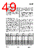
49 / 100 page  CC1100 SWRS038D Page 49 of 92 23 Voltage Regulators CC1100 contains several on-chip linear voltage regulators, which generate the supply voltage needed by low-voltage modules. These voltage regulators are invisible to the user, and can be viewed as integral parts of the various modules. The user must however make sure that the absolute maximum ratings and required pin voltages in Table 1 and Table 13 are not exceeded. The voltage regulator for the digital core requires one external decoupling capacitor. Setting the CSn pin low turns on the voltage regulator to the digital core and starts the crystal oscillator. The SO pin on the SPI interface must go low before the first positive edge of SCLK. (setup time is given in Table 16). If the chip is programmed to enter power-down mode, (SPWD strobe issued), the power will be turned off after CSn goes high. The power and crystal oscillator will be turned on again when CSn goes low. The voltage regulator output should only be used for driving the CC1100. 24 Output Power Programming The RF output power level from the device has two levels of programmability, as illustrated in Figure 22. Firstly, the special PATABLE register can hold up to eight user selected output power settings. Secondly, the 3-bit FREND0.PA_POWER value selects the PATABLE entry to use. This two-level functionality provides flexible PA power ramp up and ramp down at the start and end of transmission, as well as ASK modulation shaping. All the PA power settings in the PATABLE from index 0 up to the FREND0.PA_POWER value are used. The power ramping at the start and at the end of a packet can be turned off by setting FREND0.PA_POWER to zero and then program the desired output power to index 0 in the PATABLE. If OOK modulation is used, the logic 0 and logic 1 power levels shall be programmed to index 0 and 1 respectively. Table 30 contains recommended PATABLE settings for various output levels and frequency bands. Using PA settings from 0x61 to 0x6F is not recommended. See Section 10.6 on page 28 for PATABLE programming details. Table 31 contains output power and current consumption for default PATABLE setting (0xC6). PATABLE must be programmed in burst mode if you want to write to other entries than PATABLE[0]. Note that all content of the PATABLE, except for the first byte (index 0) is lost when entering the SLEEP state. 315 MHz 433 MHz 868 MHz 915 MHz Output Power [dBm] Setting Current Consumption, Typ. [mA] Setting Current Consumption, Typ. [mA] Setting Current Consumption, Typ. [mA] Setting Current Consumption, Typ. [mA] -30 0x04 10.6 0x04 11.5 0x03 11.9 0x11 11.8 -20 0x17 11.1 0x17 12.1 0x0D 12.4 0x0D 12.3 -15 0x1D 11.8 0x1C 12.7 0x1C 13.0 0x1C 13.0 -10 0x26 13.0 0x26 14.0 0x34 14.5 0x26 14.3 -5 0x57 12.9 0x57 13.7 0x57 14.1 0x57 13.9 0 0x60 14.8 0x60 15.6 0x8E 16.9 0x8E 16.7 5 0x85 18.1 0x85 19.1 0x85 20.0 0x83 19.9 7 0xCB 22.1 0xC8 24.2 0xCC 25.8 0xC9 25.8 10 0xC2 27.1 0xC0 29.2 0xC3 31.1 0xC0 32.3 Table 30: Optimum PATABLE Settings for Various Output Power Levels and Frequency Bands |
|
Link URL |
| Does ALLDATASHEET help your business so far? [ DONATE ] |
About Alldatasheet | Advertisement | Contact us | Privacy Policy | Link to Datasheet | Link Exchange | Manufacturer List All Rights Reserved©Alldatasheet.com |
| Russian : Alldatasheetru.com | Korean : Alldatasheet.co.kr | Spanish : Alldatasheet.es | French : Alldatasheet.fr | Italian : Alldatasheetit.com Portuguese : Alldatasheetpt.com | Polish : Alldatasheet.pl | Vietnamese : Alldatasheet.vn Indian : Alldatasheet.in | Mexican : Alldatasheet.com.mx | British : Alldatasheet.co.uk | New Zealand : Alldatasheet.co.nz |
|
Family Site : ic2ic.com |
icmetro.com |
 English ▼
 English
 Chinese
 German
 Japanese
 Russian
 Korean
 Spanish
 French
 Italian
 Portuguese
 Polish
 Vietnamese
 Indian
 Mexican
 British
 New Zealand