|
Electronic Components Datasheet Search |
|
|
Electronic Components Datasheet Search |
|
CC1100-RTY1 Datasheet(PDF) 44 Page - Texas Instruments |
|
|
|
|||||||||||||||||||||||||||||
CC1100-RTY1 Datasheet(HTML) 44 Page - Texas Instruments |
|
|
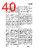
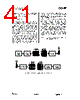
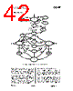
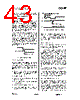
44 / 100 page  CC1100 SWRS038D Page 44 of 92 low again will turn on the regulator and crystal oscillator and make the chip enter the IDLE state. When wake on radio is enabled, the WOR module will control the voltage regulator as described in Section 19.5. 19.4 Active Modes CC1100 has two active modes: receive and transmit. These modes are activated directly by the MCU by using the SRX and STX command strobes, or automatically by Wake on Radio. The frequency synthesizer must be calibrated regularly. CC1100 has one manual calibration option (using the SCAL strobe), and three automatic calibration options, controlled by the MCSM0.FS_AUTOCAL setting: • Calibrate when going from IDLE to either RX or TX (or FSTXON) • Calibrate when going from either RX or TX to IDLE automatically • Calibrate every fourth time when going from either RX or TX to IDLE automatically If the radio goes from TX or RX to IDLE by issuing an SIDLE strobe, calibration will not be performed. The calibration takes a constant number of XOSC cycles (see Table 28 for timing details). When RX is activated, the chip will remain in receive mode until a packet is successfully received or the RX termination timer expires (see Section 19.7). Note: the probability that a false sync word is detected can be reduced by using PQT, CS, maximum sync word length, and sync word qualifier mode as described in Section 17. After a packet is successfully received the radio controller will then go to the state indicated by the MCSM1.RXOFF_MODE setting. The possible destinations are: • IDLE • FSTXON: Frequency synthesizer on and ready at the TX frequency. Activate TX with STX . • TX: Start sending preamble • RX: Start search for a new packet Similarly, when TX is active the chip will remain in the TX state until the current packet has been successfully transmitted. Then the state will change as indicated by the MCSM1.TXOFF_MODE setting. The possible destinations are the same as for RX. The MCU can manually change the state from RX to TX and vice versa by using the command strobes. If the radio controller is currently in transmit and the SRX strobe is used, the current transmission will be ended and the transition to RX will be done. If the radio controller is in RX when the STX or SFSTXON command strobes are used, the TX- if-CCA function will be used. If the channel is not clear, the chip will remain in RX. The MCSM1.CCA_MODE setting controls the conditions for clear channel assessment. See Section 17.5 on page 40 for details. The SIDLE command strobe can always be used to force the radio controller to go to the IDLE state. 19.5 Wake On Radio (WOR) The optional Wake on Radio (WOR) functionality enables CC1100 to periodically wake up from SLEEP and listen for incoming packets without MCU interaction. When the WOR strobe command is sent on the SPI interface, the CC1100 will go to the SLEEP state when CSn is released. The RC oscillator must be enabled before the WOR strobe can be used, as it is the clock source for the WOR timer. The on-chip timer will set CC1100 into IDLE state and then RX state. After a programmable time in RX, the chip will go back to the SLEEP state, unless a packet is received. See Figure 19 and Section 19.7 for details on how the timeout works. Set the CC1100 into the IDLE state to exit WOR mode. CC1100 can be set up to signal the MCU that a packet has been received by using the GDO pins. If a packet is received, the MCSM1.RXOFF_MODE will determine the behaviour at the end of the received packet. When the MCU has read the packet, it can put the chip back into SLEEP with the SWOR strobe from the IDLE state. The FIFO will loose its contents in the SLEEP state. The WOR timer has two events, Event 0 and Event 1. In the SLEEP state with WOR activated, reaching Event 0 will turn on the digital regulator and start the crystal oscillator. Event 1 follows Event 0 after a programmed timeout. |
|
Link URL |
| Does ALLDATASHEET help your business so far? [ DONATE ] |
About Alldatasheet | Advertisement | Contact us | Privacy Policy | Link to Datasheet | Link Exchange | Manufacturer List All Rights Reserved©Alldatasheet.com |
| Russian : Alldatasheetru.com | Korean : Alldatasheet.co.kr | Spanish : Alldatasheet.es | French : Alldatasheet.fr | Italian : Alldatasheetit.com Portuguese : Alldatasheetpt.com | Polish : Alldatasheet.pl | Vietnamese : Alldatasheet.vn Indian : Alldatasheet.in | Mexican : Alldatasheet.com.mx | British : Alldatasheet.co.uk | New Zealand : Alldatasheet.co.nz |
|
Family Site : ic2ic.com |
icmetro.com |
 English ▼
 English
 Chinese
 German
 Japanese
 Russian
 Korean
 Spanish
 French
 Italian
 Portuguese
 Polish
 Vietnamese
 Indian
 Mexican
 British
 New Zealand