|
Electronic Components Datasheet Search |
|
|
Electronic Components Datasheet Search |
|
CC1100-RTY1 Datasheet(PDF) 64 Page - Texas Instruments |
|
|
|
|||||||||||||||||||||||||||||
CC1100-RTY1 Datasheet(HTML) 64 Page - Texas Instruments |
|
|
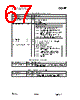
64 / 100 page  CC1100 SWRS038D Page 64 of 92 33.1 Configuration Register Details – Registers with preserved values in SLEEP state 0x00: IOCFG2 – GDO2 Output Pin Configuration Bit Field Name Reset R/W Description 7 Reserved R0 6 GDO2 _INV 0 R/W Invert output, i.e. select active low (1) / high (0) 5:0 GDO2 _CFG[5:0] 41 (0x29) R/W Default is CHP_RDYn (See Table 34 on page 56). 0x01: IOCFG1 – GDO1 Output Pin Configuration Bit Field Name Reset R/W Description 7 GDO_DS 0 R/W Set high (1) or low (0) output drive strength on the GDO pins. 6 GDO1 _INV 0 R/W Invert output, i.e. select active low (1) / high (0) 5:0 GDO1 _CFG[5:0] 46 (0x2E) R/W Default is 3-state (See Table 34 on page 56). 0x02: IOCFG0 – GDO0 Output Pin Configuration Bit Field Name Reset R/W Description 7 TEMP_SENSOR_ENABLE 0 R/W Enable analog temperature sensor. Write 0 in all other register bits when using temperature sensor. 6 GDO0 _INV 0 R/W Invert output, i.e. select active low (1) / high (0) 5:0 GDO0 _CFG[5:0] 63 (0x3F) R/W Default is CLK_XOSC/192 (See Table 34 on page 56). It is recommended to disable the clock output in initialization, in order to optimize RF performance. |
|
Link URL |
| Does ALLDATASHEET help your business so far? [ DONATE ] |
About Alldatasheet | Advertisement | Contact us | Privacy Policy | Link to Datasheet | Link Exchange | Manufacturer List All Rights Reserved©Alldatasheet.com |
| Russian : Alldatasheetru.com | Korean : Alldatasheet.co.kr | Spanish : Alldatasheet.es | French : Alldatasheet.fr | Italian : Alldatasheetit.com Portuguese : Alldatasheetpt.com | Polish : Alldatasheet.pl | Vietnamese : Alldatasheet.vn Indian : Alldatasheet.in | Mexican : Alldatasheet.com.mx | British : Alldatasheet.co.uk | New Zealand : Alldatasheet.co.nz |
|
Family Site : ic2ic.com |
icmetro.com |
 English ▼
 English
 Chinese
 German
 Japanese
 Russian
 Korean
 Spanish
 French
 Italian
 Portuguese
 Polish
 Vietnamese
 Indian
 Mexican
 British
 New Zealand