|
Electronic Components Datasheet Search |
|
|
Electronic Components Datasheet Search |
|
LPC2921 Datasheet(PDF) 35 Page - NXP Semiconductors |
|
|
|||||||||||||||||||||||||||||
LPC2921 Datasheet(HTML) 35 Page - NXP Semiconductors |
|
|
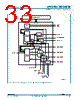
35 / 81 page  LPC2921_2923_2925_0 © NXP B.V. 2008. All rights reserved. Preliminary data sheet Rev. 00.01 — 24 October 2008 35 of 81 NXP Semiconductors LPC2921/2923/2925 ARM9 microcontroller with CAN and LIN 6.14.4.1 Functional description The ADC block diagram, Figure 6, shows the basic architecture of each ADC. The ADC functionality is divided into two major parts; one part running on the MSCSS Subsystem clock, the other on the ADC clock. This split into two clock domains affects the behavior from a system-level perspective. The actual analog-to-digital conversions take place in the ADC clock domain, but system control takes place in the system clock domain. A mechanism is provided to modify configuration of the ADC and control the moment at which the updated configuration is transferred to the ADC domain. The ADC clock is limited to 4.5 MHz maximum frequency and should always be lower than or equal to the system clock frequency. To meet this constraint or to select the desired lower sampling frequency, the clock generation unit provides a programmable fractional system-clock divider dedicated to the ADC clock. Conversion rate is determined by the ADC clock frequency divided by the number of resolution bits plus one. Accessing ADC registers requires an enabled ADC clock, which is controllable via the clock generation unit, see Section 6.15.2. Each ADC has four start inputs. Note that start 0 and start 2 are captured in the system clock domain while start 1 and start 3 are captured in the ADC domain. The start inputs are connected at MSCSS level, see Section 6.14 for details. 6.14.4.2 Pin description The two ADC modules in the MSCSS have the pins described below. The ADCx input pins are combined with other functions on the port pins of the LPC2921/2923/2925. The VREFN and VREFP pins are common for both ADCs. Table 20 shows the ADC pins. Fig 6. ADC block diagram 002aae251 ADC start 2 ADC start 0 APB clock (BASE_MSCSS_CLK) ADC clock (up to 4.5 MHz) (BASE_ADC_CLK) APB system bus IRQ scan IRQ compare ADC2 IN[7:0] ADC start 1 ADC start 3 sync_out ADC DOMAIN SYSTEM DOMAIN ADC CONTROL ADC REGISTERS 3.3 V ADC2 3.3 V ADC1 ANALOG MUX conversion data update configuration data IRQ ADC1 IN[7:0] ANALOG MUX 3.3 V IN 3.3 V IN |
|
Link URL |
| Does ALLDATASHEET help your business so far? [ DONATE ] |
About Alldatasheet | Advertisement | Contact us | Privacy Policy | Link to Datasheet | Link Exchange | Manufacturer List All Rights Reserved©Alldatasheet.com |
| Russian : Alldatasheetru.com | Korean : Alldatasheet.co.kr | Spanish : Alldatasheet.es | French : Alldatasheet.fr | Italian : Alldatasheetit.com Portuguese : Alldatasheetpt.com | Polish : Alldatasheet.pl | Vietnamese : Alldatasheet.vn Indian : Alldatasheet.in | Mexican : Alldatasheet.com.mx | British : Alldatasheet.co.uk | New Zealand : Alldatasheet.co.nz |
|
Family Site : ic2ic.com |
icmetro.com |
 English ▼
 English
 Chinese
 German
 Japanese
 Russian
 Korean
 Spanish
 French
 Italian
 Portuguese
 Polish
 Vietnamese
 Indian
 Mexican
 British
 New Zealand